Semiconductor integrated circuit device with power-on reset circuit for detecting the operating state of an analog circuit

Inactive Publication Date: 2007-01-04
KK TOSHIBA
View PDF4 Cites 5 Cited by
  • Summary
  • Abstract
  • Description
  • Claims
  • Application Information

AI Technical Summary

Benefits of technology

[0011] a check circuit which checks the operating state of an analog circuit which carries out an analog operation using the first power supply and outputs a control signal indicating whether the analog circuit is operating properly, a detecting level of the first detecting circuit b

Problems solved by technology

However, even if a conventional detecting circuit has sensed that the power supply has reached a sufficient voltage level for the operation of the logic circuit, the voltage level might not be sufficient for the operation of the analog circuit.
In such a case, the logic circuit operates properly, but the analog circuit operates erroneously.

Method used


Image

  • Semiconductor integrated circuit device with power-on reset circuit for detecting the operating state of an analog circuit
  • Semiconductor integrated circuit device with power-on reset circuit for detecting the operating state of an analog circuit
  • Semiconductor integrated circuit device with power-on reset circuit for detecting the operating state of an analog circuit

Examples


first embodiment

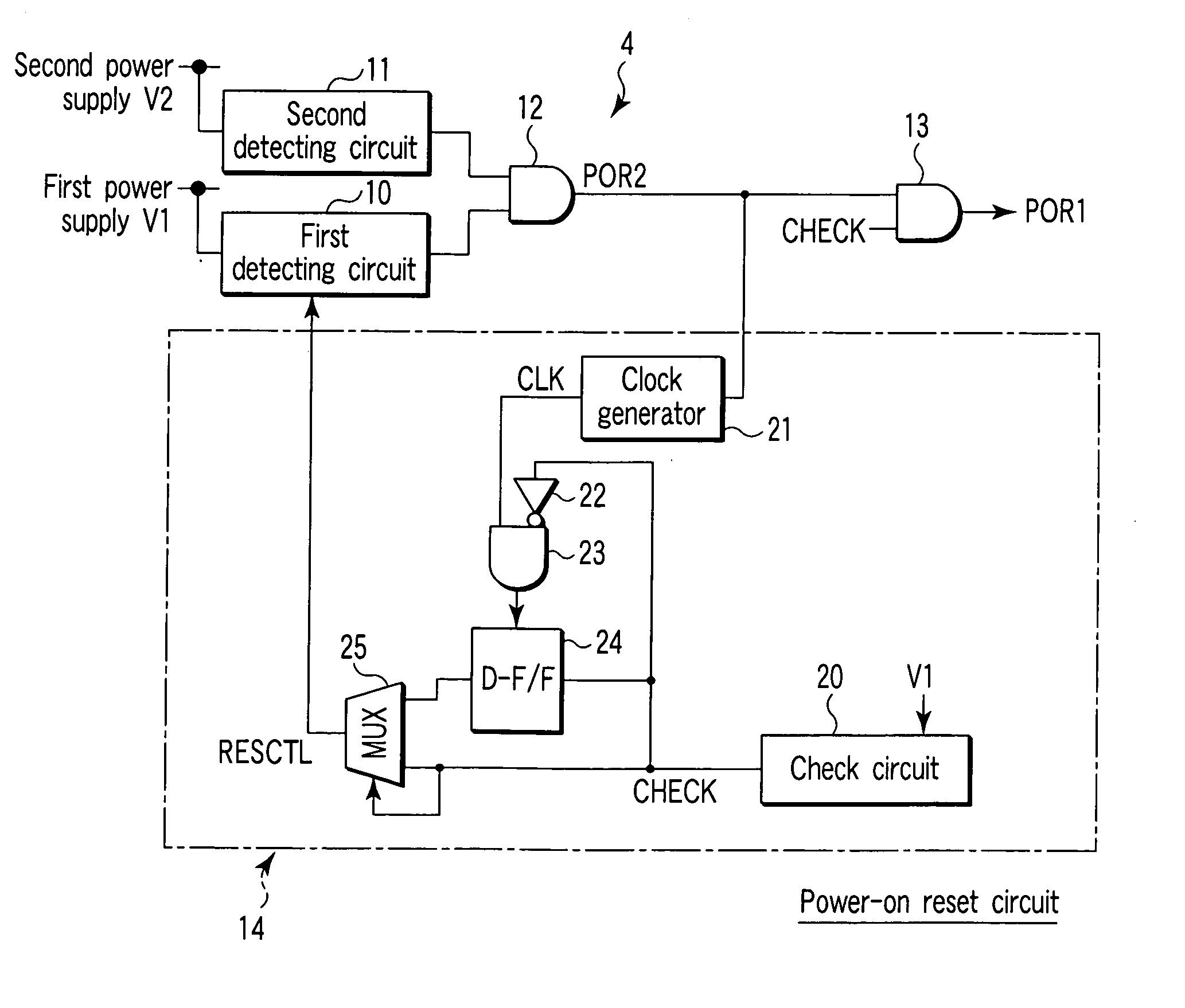
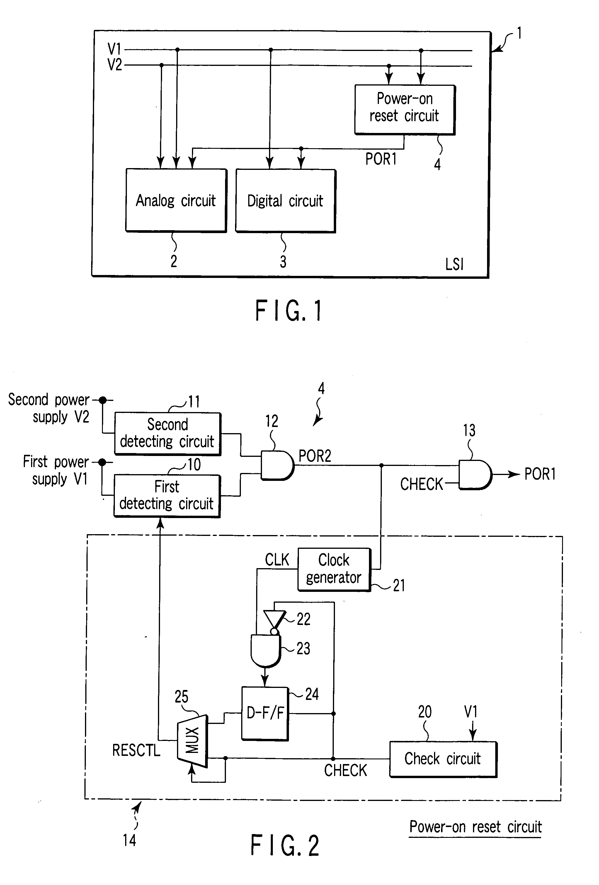
[0042] As shown in FIG. 1, an LSI 1 of the first embodiment comprises an analog circuit 2, a digital circuit 3, and a power-on reset circuit 4. The analog circuit 2, which carries out an analog operation, uses a first power supply V1 (e.g., 1.5 V) and a second power supply V2 (|V2|>|V1|) as power supply voltages. The digital circuit 3, which carries out a digital operation, uses the first power supply V1 as a power supply voltage. The power-on reset circuit 4 senses whether each of the first and second power supplies V1 and V2 has reached a specific value. When they have reached the respective specific values, the power-on reset circuit 4 asserts a power-on reset signal POR1 (or sets a power-on reset signal POR1 to a high (H) level). When the power-on reset signal POR1 is asserted, the analog circuit 2 and digital circuit 3 go into an operable state.

[0043]FIG. 2 is a circuit diagram of the power-on reset circuit 4. As shown in FIG. 2, the power-on reset circuit 4 includes a first de...

second embodiment

[0088] The configuration produces the effect in the following item (3) in addition to the effects in item (1) and item (2)

[0089] (3) The detecting level can be set more accurately.

[0090] In the second embodiment, the control circuit 14 of the power-on reset circuit 4 includes the shift register 28 which holds an (n+1)-bit level control signal RESCTL [0:n]. The variable resistive element 51 of the first detecting circuit 10 includes an n number of resistive elements 56-1 to 56-n and an n number of MOS transistors 56-1 to 56-n. The individual bits in the level control signal RESCTL [0:n] are allocated to the gates of the MOS transistors 55, 56-1 to 56-n, respectively. Therefore, the resistance of the variable resistive element 51, or the reference voltage Vref1 can be set to a plurality of values (e.g., (n+1) values). As described above, since the reference voltage Vref1 can be fine-tuned, enabling the necessary detecting level to be set accurately, which helps prevent the first pow...

third embodiment

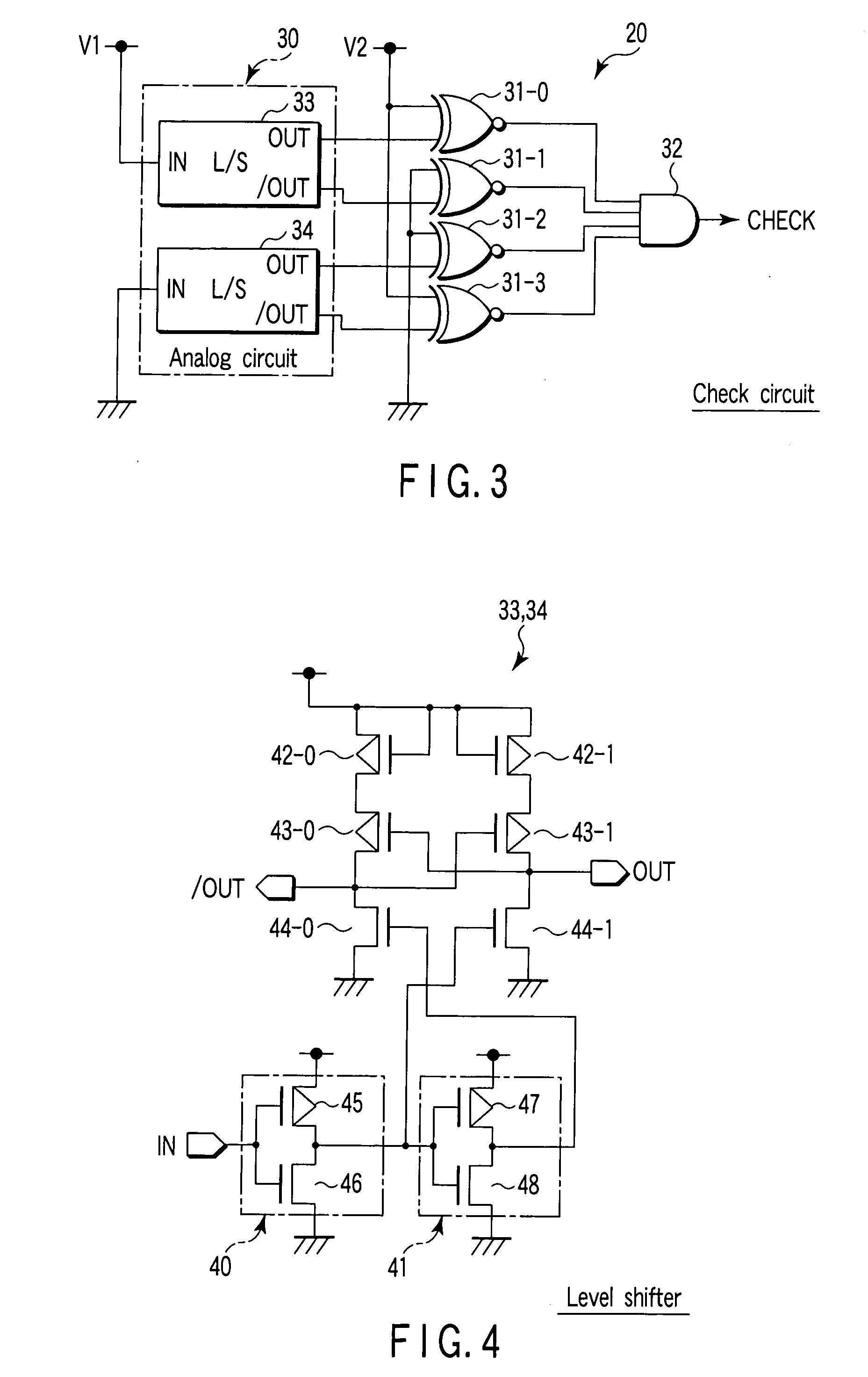
[0092]FIG. 11 is a circuit diagram of the power-on reset circuit 4 according to the As shown in FIG. 11, the check circuit 20 includes a dummy fuse block 35 and a read check circuit 36. The dummy fuse block, which includes a fuse element, has the same configuration as that of the fuse circuit included in, for example, the analog circuit 2. The read check circuit 36 reads the data from the dummy fuse block. When having carried out the reading operation properly, the read check circuit 36 asserts the detect signal CHECK.

[0093] As described above, the dummy fuse block is used as the analog circuit 30 in place of the level shifter. Even when a failure in the analog circuit in the dummy fuse block has been detected, the same operation as in the first embodiment can be performed, which produces the same effects as those in item (1) and item (2).

[0094] Next, a semiconductor integrated circuit according to a fourth embodiment of the present invention will be explained. The fourth embodime...


PUM


Abstract

A semiconductor integrated circuit device operates using a first power supply and a second power supply differing from the first power supply in voltage. The semiconductor integrated circuit device includes a first detecting circuit which detects that the first power supply has exceeded a specific voltage, a second detecting circuit which detects that the second power supply has exceeded a specific voltage, and a check circuit which checks the operating state of an analog circuit carrying out an analog operation using the first power supply and outputs a control signal indicating whether the analog circuit is operating properly. The detecting level of the first detecting circuit is determined on the basis of the control signal. A power-on reset signal is output according to the result of the detection at the first and second detecting circuits.

Description

CROSS-REFERENCE TO RELATED APPLICATIONS [0001] This application is based upon and claims the benefit of priority from prior Japanese Patent Application No. 2005-189951, filed Jun. 29, 2005, the entire contents of which are incorporated herein by reference. BACKGROUND OF THE INVENTION [0002] 1. Field of the Invention [0003] This invention relates to a semiconductor integrated circuit device. More particularly, this invention relates to a semiconductor integrated circuit device which has a semiconductor memory device and a logic circuit formed on a single semiconductor substrate. [0004] 2. Description of the Related Art [0005] In the field of a semiconductor integrated circuit (LSI) which has a semiconductor memory and a logic circuit formed on a single substrate, the need for a rewritable flash memory as a semiconductor memory has recently being increasing. [0006] In a combined flash memory / logic LSI, a low-voltage power supply is used in the logic circuit to meet low-power requireme...

Claims


Application Information

Patent Timeline
IPC IPC(8): H02J1/10
CPCG11C5/143G11C16/0433H03K17/22G11C16/30G11C16/225
Inventor KAMOSHIDA, MASAHIRO
Owner KK TOSHIBA
Why Eureka
Try Eureka