Light emitting display device and method for driving the same

a technology of light-emitting display and display device, which is applied in the direction of static indicating device, electroluminescent light source, instruments, etc., can solve the problems of large restriction, inability to unconditionally make the mirror ratio large, and hampered the charging speed of the data line, so as to minimize the variation in voltage

Active Publication Date: 2007-01-04
LG DISPLAY CO LTD
View PDF6 Cites 4 Cited by
  • Summary
  • Abstract
  • Description
  • Claims
  • Application Information

AI Technical Summary

Benefits of technology

[0022] An advantage of the present invention is to provide a light emitting display device that is capable of supplying a first voltage to a first TFT and a voltage resulting from division of the first voltage and a second voltage to a second TFT, respectively, such that the voltage to the second TFT varies with the first voltage, thereby minimizing a variation in the voltage between the gate electrode and source electrode of the first TFT, and a method for driving the same.
[0023] Additional features and advantages of the invention will be set forth in the description which follows, and in part will be apparent from the description, or may be learned from practice of the invention. The objectives and other advantages of the invention may be realized and attained by the structure particularly pointed out in the written description and claims hereof as well as the appended drawings.
[0024] To achieve these and other advantages and in accordance with the purpose of the invention, as embodied and broadly described, a light emitting display device may include a display unit having a plurality of pixels defined by a plurality of gate lines and a plurality of data lines, each of the pixels including: a light emitting element that emits light in response to a drive current based on a gray-scale current on the associated data line; a first switching element that supplies the drive current to the light emitting element; a second switching element connected with the first switching element that forms a current mirror with the first switching element; a first voltage line that supplies a first voltage to the first switching element; a second voltage line that supplies a second voltage to the second switching element; and a voltage supply circuit that divides the first voltage from the first voltage line and the second voltage from the second voltage line and supplies the resulting voltage to a source electrode of the second switching element.
[0025] In another aspect of the present invention, a method for driving a light emitting display device, where the light emitting display device includes a display unit having a plurality of pixels defined by a plurality of gate lines and a plurality of data lines, each of the pixels including a light emitting element that emits light in response to drive current based on a gray-scale current on an associated one of the data lines, a first switching element that supplies the drive current to the light emitting element, a second switching element connected with the first switching element that forms a current mirror with the first switching element, a first voltage line that supplies a first voltage to the first switching element, and a second voltage line that supplies a second voltage to the second switching element, a third switching element for forming a short circuit between a gate electrode and drain electrode of the second switching element in response to a scan pulse from an associated one of the gate lines, a fourth switching element for connecting the second switching element with the associated data line in response to the scan pulse from the associated gate line, includes: dividing the first voltage from the first voltage line and the second voltage from the second voltage line; and supplying the divided voltage to a source electrode of the second switching element.
[0026] It is to be understood that both the foregoing general description and the following detailed description of the present invention are exemplary and explanatory and are intended to provide further explanation of the invention as claimed.

Problems solved by technology

However, the mirror ratio is greatly restricted by a TFT design constraints.
For this reason, it is not possible to unconditionally make the mirror ratio large.
As a result, increasing the charging speed of the data line is still hampered by a big restriction.
In particular, the distortion of the first voltage VDD1 from the first voltage line VL1 becomes a big issue, because the first voltage VDD1 is related to drive current to be supplied to the light emitting element OLED.

Method used


Image

  • Light emitting display device and method for driving the same
  • Light emitting display device and method for driving the same
  • Light emitting display device and method for driving the same

Examples


first embodiment

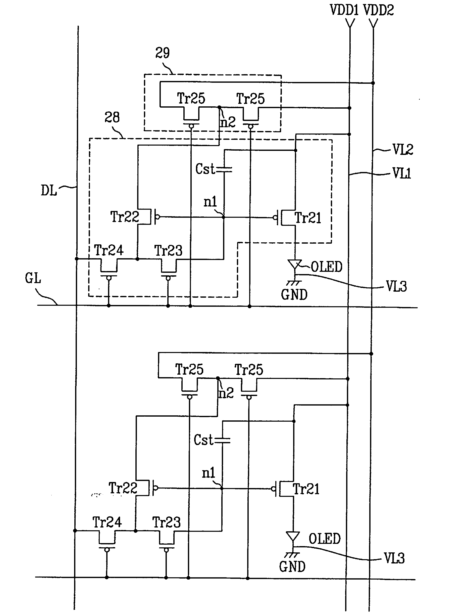
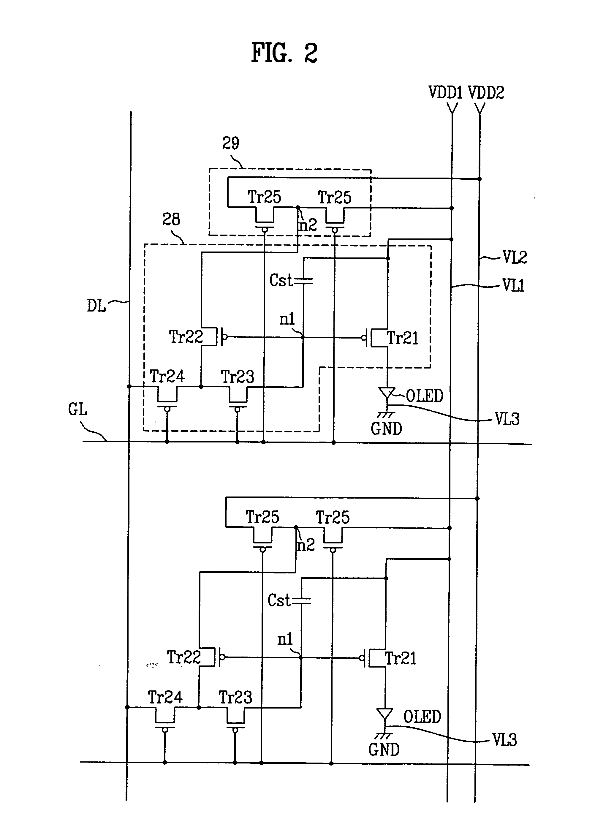
[0035]FIG. 2 shows the structure of two pixels in a light emitting display device according to the present invention.

[0036] The light emitting display device according to the first embodiment of the present invention includes a display unit (not shown) that has a plurality of pixels defined by a plurality of gate lines GL and a plurality of data lines DL crossing each other substantially perpendicularly, as shown in FIG. 2.

[0037] Each pixel includes a first voltage line VL1 for supplying a first voltage VDD1, a second voltage line VL2 for supplying a second voltage VDD2, a pixel circuit 28 connected to the associated data line DL and gate line GL, a light emitting element OLED connected between the pixel circuit 28 and a third voltage line VL3 which supplies a third voltage GND, and a voltage supply circuit 29 for dividing the first voltage VDD1 from the first voltage line VL1 and the second voltage VDD2 from the second voltage line VL2 and supplying the resulting voltage to the pi...

second embodiment

[0055] Next, a detailed description will be given of a light emitting display device according to the present invention.

[0056]FIG. 3 shows the structure of two pixels in the light emitting display device according to the second embodiment of the present invention.

[0057] The light emitting display device according to the second embodiment is substantially the same in configuration as the above-described light emitting display device according to the first embodiment, with the exception that a voltage supply circuit 39 is different from the voltage supply circuit 29, as shown in FIG. 3.

[0058] The voltage supply circuit 39 of the light emitting display device according to the second embodiment of the present invention includes a plurality of fifth TFTs Tr35, as shown in FIG. 3. The fifth TFTs Tr35 are connected in series between the first voltage line VL1 and the second voltage line VL2. Each of the fifth TFTs Tr35 has a diode structure where the gate electrode and drain electrode th...

third embodiment

[0060] Next, a detailed description will be given of a light emitting display device according to the present invention.

[0061]FIG. 4 shows the structure of two pixels in the light emitting display device according to the third embodiment of the present invention.

[0062] The light emitting display device according to the third embodiment is substantially the same in configuration as the above-described light emitting display device according to the first embodiment, with the exception that a voltage supply circuit 49 is different from the voltage supply circuit 29, as shown in FIG. 4.

[0063] The voltage supply circuit 49 of the light emitting display device according to the third embodiment of the present invention includes a plurality of fifth TFTs Tr45, as shown in FIG. 4. The fifth TFTs Tr45 are connected in series between the first voltage line VL1 and the second voltage line VL2. The fifth TFTs Tr45 have their respective gate electrodes connected in common to the source electrod...


PUM


Abstract

A light emitting display device and a method for driving the same are disclosed. Each pixel of the light emitting display device includes: a light emitting element that emits light in response to a drive current based on a gray-scale current on the associated data line; a first switching element that supplies the drive current to the light emitting element; a first voltage line that supplies a first voltage to a source electrode of the first switching element; a second switching element connected with the first switching element that forms a current mirror with the first switching element; a second voltage line that supplies a second voltage of the second switching element; and a voltage supply circuit that divides the first voltage from the first voltage line and the second voltage from the second voltage line and supplyies the resulting voltage to a source electrode of the second switching element.

Description

[0001] This application claims the benefit of Korean Patent Application No. 10-2005-0057573, filed on Jun. 30, 2005, which is hereby incorporated by reference for all purposes as if fully set forth herein. BACKGROUND OF THE INVENTION [0002] 1. Field of the Invention [0003] The present invention relates to a light emitting display device, and more particularly, to a light emitting display device that is capable of avoiding a brightness difference between respective pixels resulting from a voltage variation, and a method for driving the same. [0004] 2. Discussion of the Related Art [0005] Recently, various flat panel display devices have been developed to reduce weight and volume which are disadvantages of a cathode ray tube. These flat panel display devices may be, for example, a liquid crystal display, a field emission display, a plasma display panel, a light emitting display, and the like. [0006] The light emitting display, among the flat panel display devices, is of a spontaneous ...

Claims


Application Information

Patent Timeline
Patent Type & Authority Applications(United States)
IPC IPC(8): G09G3/36H05B44/00
CPCG09G3/3241G09G2300/0465G09G2330/02G09G2310/0251G09G2320/0233G09G2300/0842G09G3/30
Inventor LEE, CHANG HWAN
Owner LG DISPLAY CO LTD
Why Eureka
Try Eureka