

CMOS device with dual polycide gates and method of manufacturing the same
a polysilicon layer and polycide technology, applied in the field of cmos devices, can solve the problems serious gate depletion effect, and reducing the concentration of impurities in each gate polysilicon layer quickly, and achieves the effect of increasing the short channel effect and reducing the quantity of impurities
- Summary
- Abstract
- Description
- Claims
- Application Information
AI Technical Summary
Benefits of technology
Problems solved by technology
Method used
Image

Examples
Embodiment Construction
[0035] Hereinafter, a preferred embodiment of the present invention will be described with reference to the accompanying drawings.
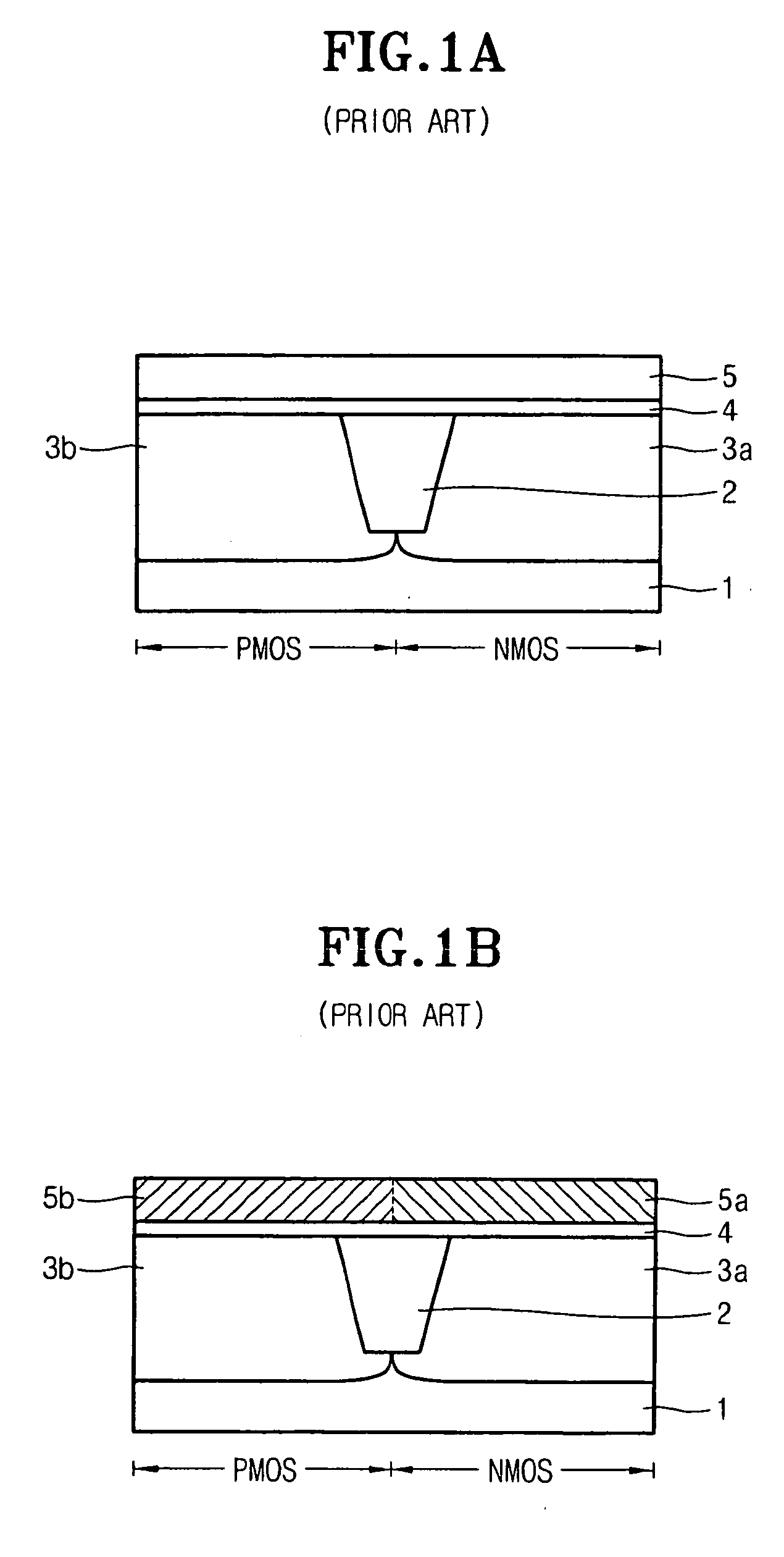
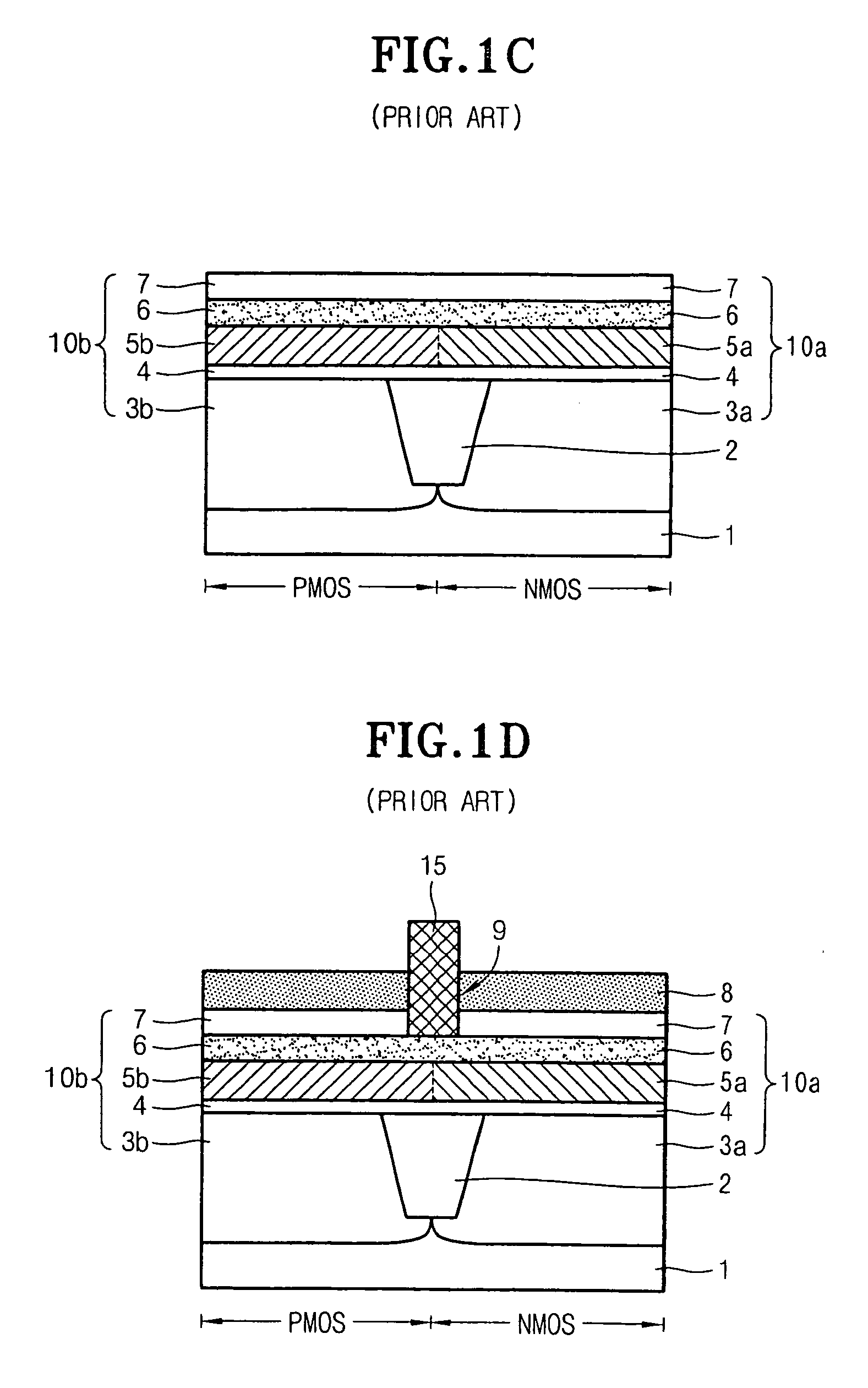
[0036]FIGS. 2A to 2D are cross-sectional views for illustrating a method of manufacturing a CMOS device according to an embodiment of the present invention, in which processes are shown step by step.
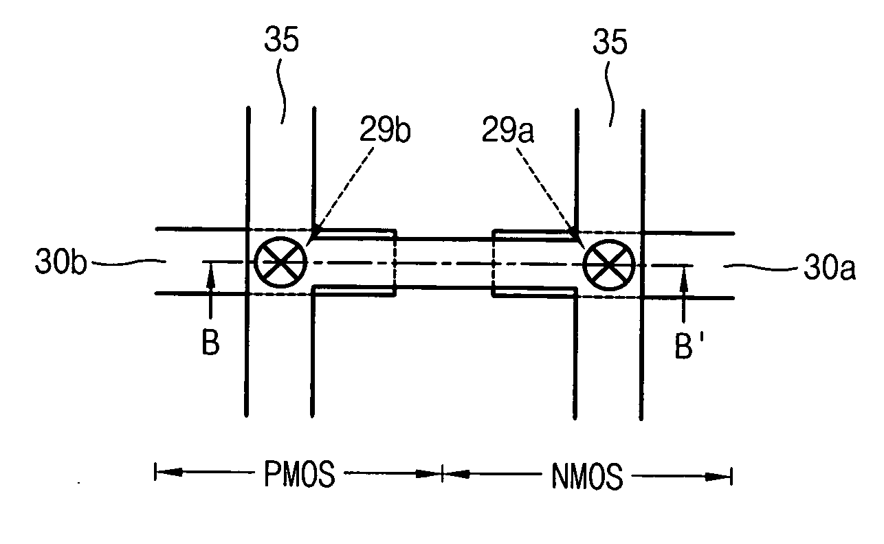
[0037] Referring to FIG. 2A, a device isolation layer 22 is formed to define an active region in each area of a silicon substrate 21 having a cell area and a peripheral circuit area, according to a shallow trench isolation process, and in turn an existing mask process and ion implantation process are performed, so as to form a P-well 23a and a N-well 23b in the peripheral circuit area of the silicon substrate 21. Thereafter, an oxide layer 24 is formed as a gate insulation layer on the silicon substrate 21 on which the device isolation layer 22, and wells 23a and 23b are formed, and then a silicon layer 25 for a gate is formed on the oxide layer 24.
[0038] H...
PUM
 Abstract
Description
Claims
Application Information