

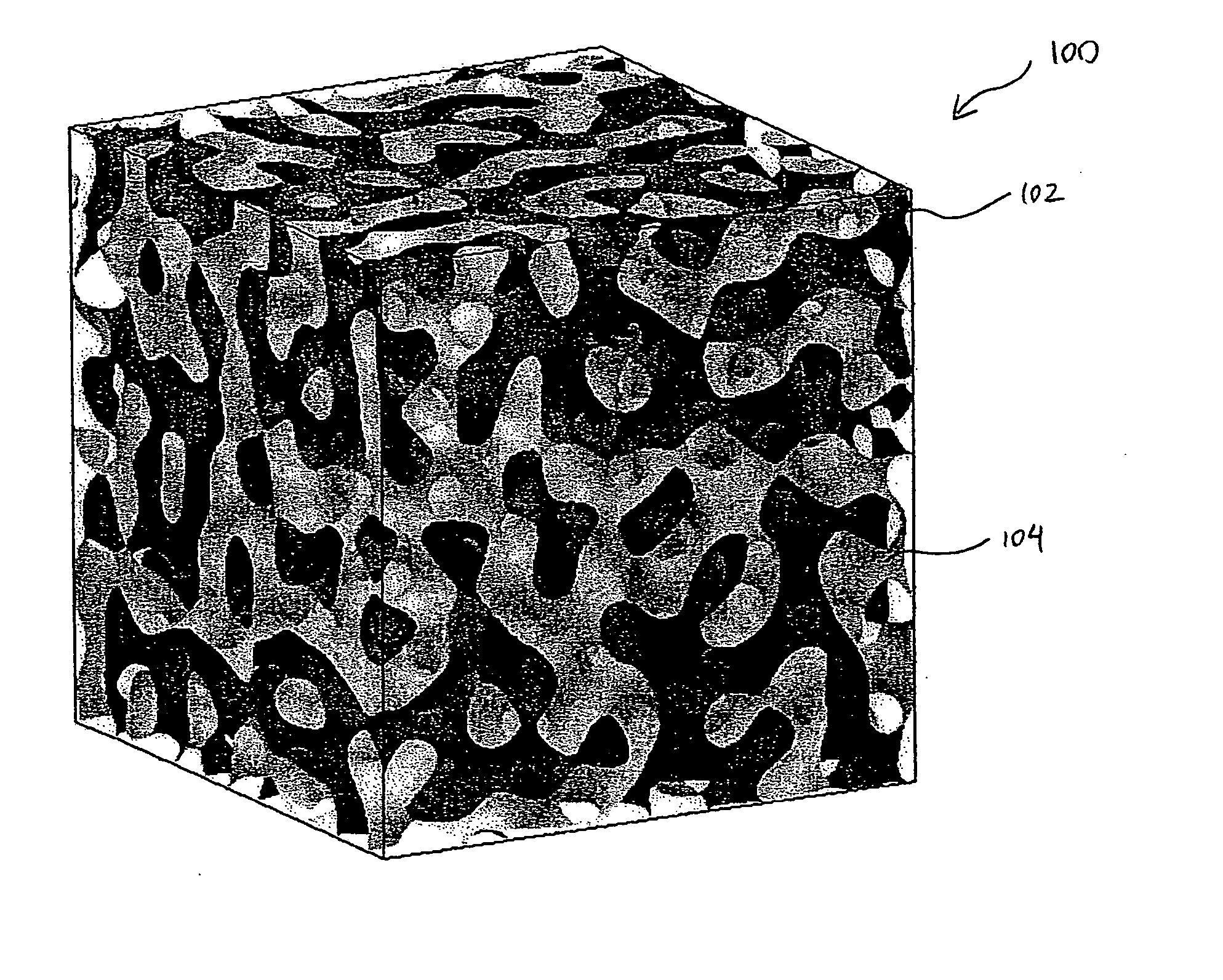
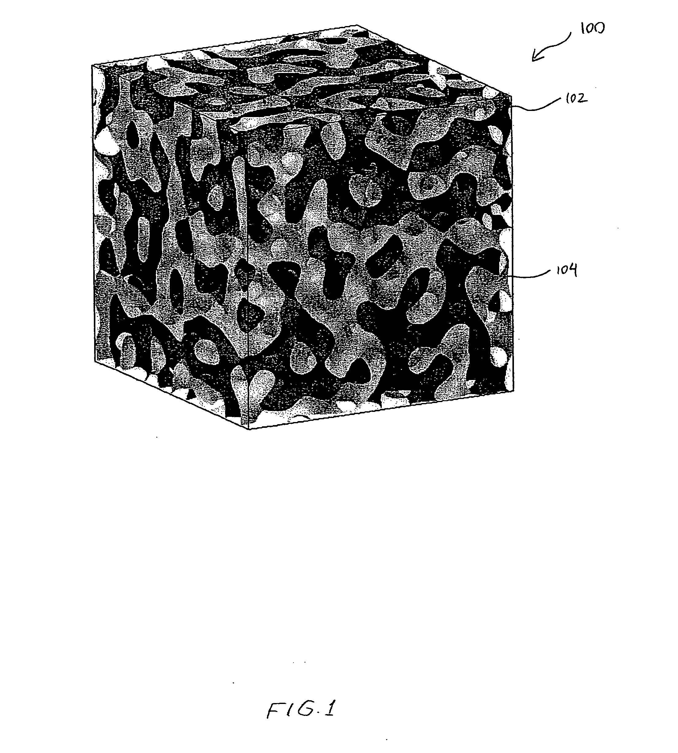
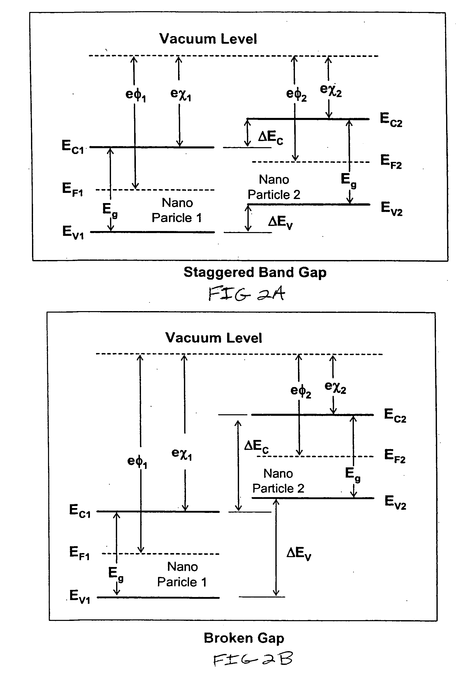
Nanostructured materials and photovoltaic devices including nanostructured materials
a nano-structured material and nano-technology, applied in the field of nano-structured materials, can solve the problems of loss or inefficiency of photovoltaic devices, inability to efficiently convert total incident light energy to useful electrical energy, and the loss of photovoltaic devices, so as to achieve the effect of efficiently converting incident light energy to useful electrical energy, and achieve the effect of reducing the cost of photovoltaic devices
- Summary
- Abstract
- Description
- Claims
- Application Information
AI Technical Summary
Benefits of technology
Problems solved by technology
Method used
Image

Examples
Embodiment Construction
Definitions
[0022] The following definitions apply to some of the elements described with regard to some embodiments of the invention. These definitions may likewise be expanded upon herein.
[0023] As used herein, the term “set” refers to a collection of one or more elements. Elements of a set can also be referred to as members of the set. Elements of a set can be the same or different. In some instances, elements of a set can share one or more common properties.
[0024] As used herein, the terms “optional” and “optionally” mean that the subsequently described event or circumstance may or may not occur and that the description includes instances where the event or circumstance occurs and instances in which it does not. For example, the phrase “optionally surrounded with a shell” means that the shell may or may not be present and that the description includes both the presence and the absence of the shell.
[0025] As used herein, the term “photoluminescence” refers to the emission of l...
PUM
 Abstract
Description
Claims
Application Information