Light-emitting device

a technology of light-emitting devices and light-emitting diodes, which is applied in the direction of lighting and heating apparatus, casings/cabinets/drawers, casings/cabinets/drawers details, etc., can solve the problems of low brightness per chip, insufficient heat generation efficiency, and deterioration of led chip life and efficiency, so as to reduce the temperature rise of light-emitting diodes and transfer heat more efficiently

Active Publication Date: 2007-01-11
MATSUSHITA ELECTRIC WORKS LTD
View PDF26 Cites 93 Cited by
  • Summary
  • Abstract
  • Description
  • Claims
  • Application Information

AI Technical Summary

Benefits of technology

[0030] It is an advantage of the invention that the heat generated in the light-emitting diode chip can be transferred easily through the thermal bonding from the submount to the first plate bonded thermally thereto.
[0031] It is another advantage of the invention that the temperature rise of the light-emitting diode chip can be decreased due to the efficient thermal transfer.
[0032] It is a further advantage of the invention that the heat generated in the light-emitting diode chip can be transferred more efficiently through a plurality of heat transfer paths to decrease the temperature of the light-emitting diode chip.

Problems solved by technology

When such a light-emitting device is used for a light source for display, a light source for liquid crystal panel or the like, the brightness per chip is low and insufficient.
It is known that characteristics such as life and efficiency of LED chip are deteriorated when the temperature rises due to the generated heat.
Because the print circuit board for mounting the LED package is generally made of a resin such as polyimide or epoxy resin having low thermal conductivity, the generated heat cannot be radiated efficiently from the LED package.
However, the above-mentioned heat transfer structure of a light emitting device has following problems.
Further, the filling step is troublesome.

Method used


Image

  • Light-emitting device
  • Light-emitting device
  • Light-emitting device

Examples


Embodiment Construction

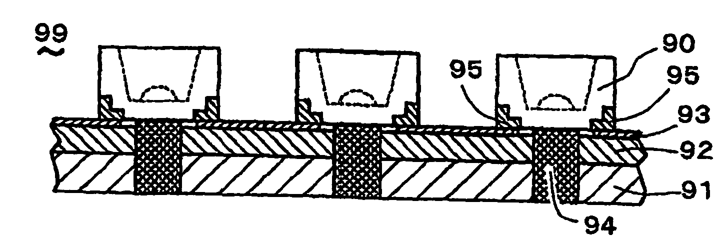
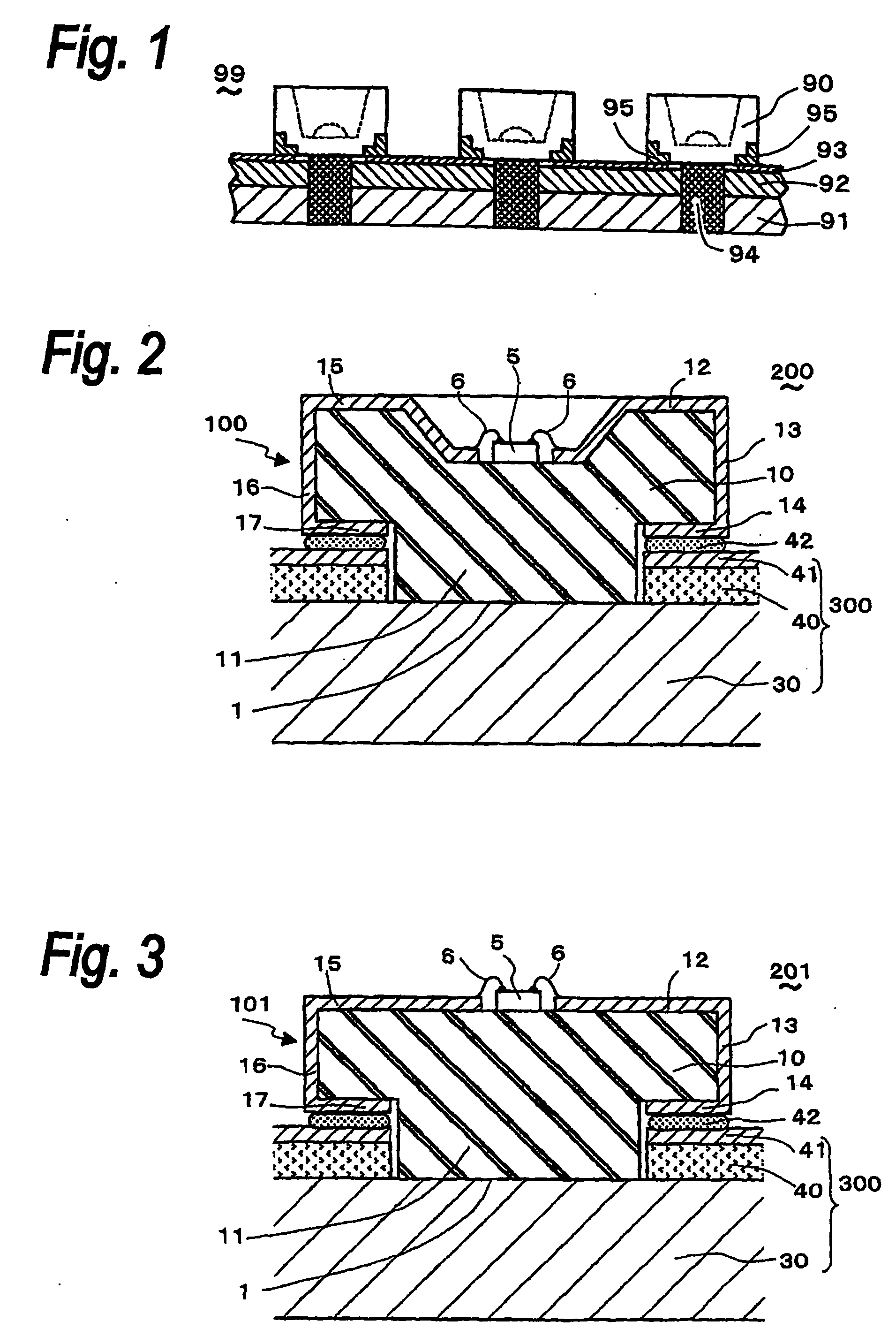
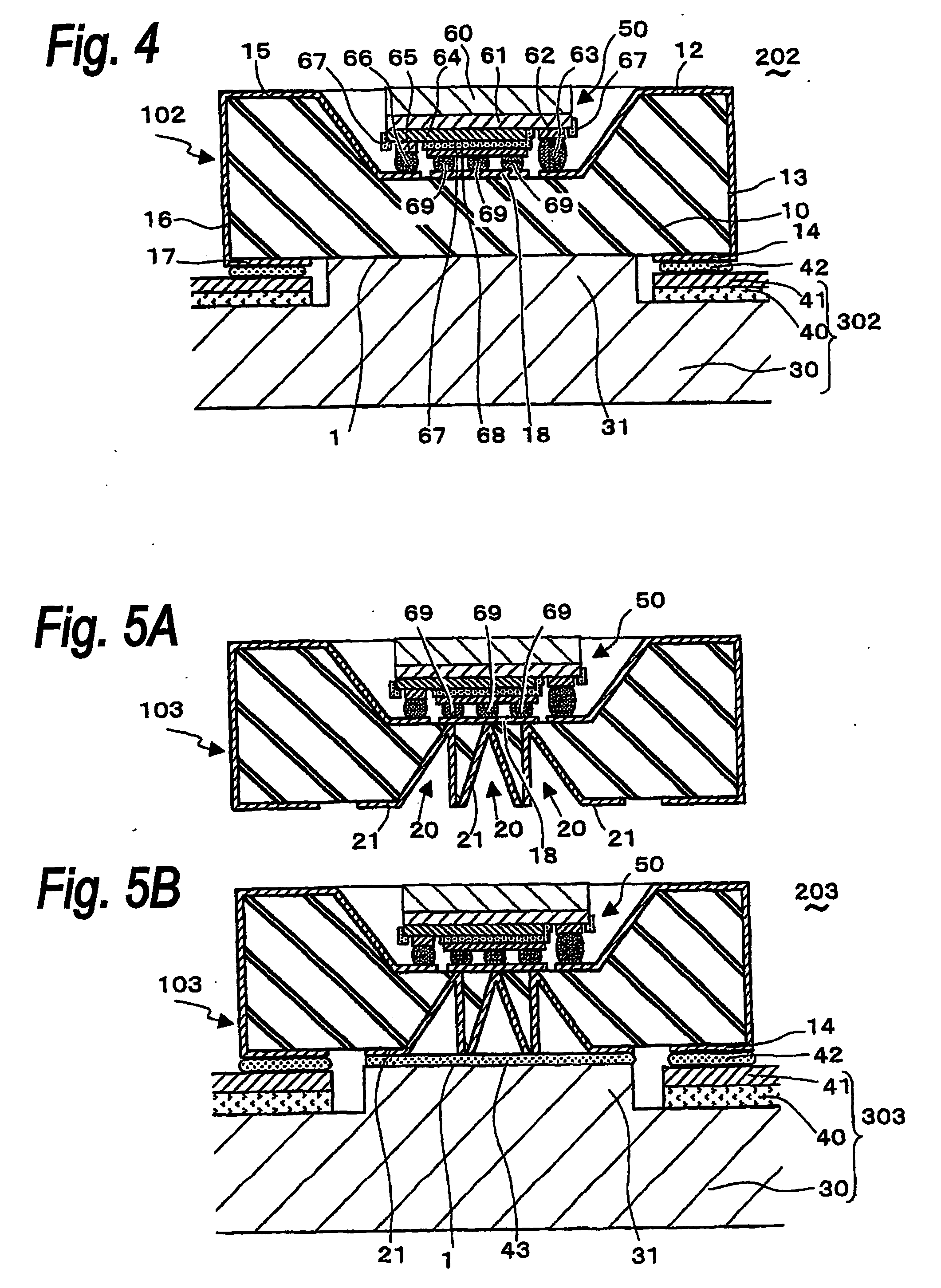
[0093] Light-emitting devices of several embodiments of the invention are explained below with reference to the appended drawings, wherein like reference characters designate like or corresponding parts throughout the several views.

[0094]FIG. 2 shows a light-emitting device 200 of an embodiment of the invention. In the light-emitting device 200, a bottom 11 of a submount 100 for LED contacts thermally with a metallic plate 30 of a circuit board 300. The submount 100 has a mount base 10 having electrically conducting lines 12-14 and 13-17 and a light-emitting diode (LED) chip 5 mounted on the mount base 10. The LED chip 5 emits a beam in a direction perpendicular to the sheet of paper on which FIG. 2 is illustrated. The circuit board 300 has the metallic plate 30 and a metallic pattern 41 for electrical conduction formed on an electrically insulating layer 40. The LED chip 5 has a gallium nitride semiconductor. In this and following embodiments, the LED chip 5 has a gallium nitride ...


PUM


Abstract

A light-emitting device (200) has a submount (100) and a plate for heat transfer (300) having a metallic plate (30). The submount (100) has a mount base (10), at least one light-emitting diode chip (5) mounted thereon and electrically conducting lines (12-17) formed on the mount base (10) to be connected electrically to the light-emitting diode chip (5). A first plane (11) of the mount base (10) of the submount (100) is bonded thermally to the first plate (300). For example, the plate is a circuit board having a metallic plate (30), and the submount (100) is bonded thermally to the metallic plate (30) of the one of the at least one plate (300). In an example, a second plate for heat transfer is also bonded thermally to a second plane of the mount base (100) for providing a plurality of heat transfer paths.

Description

TECHNICAL FIELD [0001] The invention relates to a light-emitting device having a light-emitting diode, and in particular to a light-emitting device having good heat transfer. BACKGROUND ART [0002] Recently, by combining a light-emitting diode (LED) chip for radiating blue or ultraviolet rays based on a gallium nitride semiconductor with a fluorescent material of various types, a light-emitting device which emits a light of a color or colors, including white, different from that of the emitting light of the LED chip has been developed. The light-emitting device has advantages such as small size, light weight and low dissipating power, and it is used widely for a light source for display, a light source in substitution of a small electric bulb, a light source for a liquid crystal display, and the like. When such a light-emitting device is used for a light source for display, a light source for liquid crystal panel or the like, the brightness per chip is low and insufficient. Then an L...

Claims


Application Information

Patent Timeline
Patent Type & Authority Applications(United States)
IPC IPC(8): H01L33/00H01L33/48H01L33/62H01L33/64
CPCH01L33/486H01L2924/15311H01L33/642H01L2224/48091H01L2224/48227H01L2924/01078H01L2924/01079H01L33/62H01L2924/15159H01L2924/01047H01L2924/01015H01L2924/19107H01L2224/48465H01L2224/16225H01L2224/16H01L2924/15156H01L2924/12041H01L2224/45147H01L2924/00014H01L2924/00H01L2924/15192H01L2224/05573H01L2224/05568H01L2924/00011H01L2224/16238H01L2224/17106H01L2224/17107H01L24/16H01L2224/0603H01L2224/06102H01L2224/1703H01L2224/05599H01L2924/01005H01L2924/01033
Inventor HASHIMOTO, TAKUMASUGIMOTO, MASARUYOKOTANI, RYOJINISHIOKA, KOJIIWAHORI, YUTAKAISHIZAKI, SHINYASUZUKI, TOSHIYUKIUCHINONO, YOSHIYUKIMUTO, MASAHIDEMORI, SATOSHIKIMURA, HIDEYOSHI
Owner MATSUSHITA ELECTRIC WORKS LTD
Why Eureka
Try Eureka