Supercharge Your Innovation With Domain-Expert AI Agents!

Output driver in semiconductor device

a technology of output driver and semiconductor device, which is applied in the direction of logic circuit, pulse technique, digital storage, etc., can solve the problem of difficult control of the variance of the output driver slew rate, and achieve the effect of easy control

Active Publication Date: 2007-01-11
SK HYNIX INC
View PDF10 Cites 12 Cited by
  • Summary
  • Abstract
  • Description
  • Claims
  • Application Information

AI Technical Summary

Benefits of technology

The present invention provides an output driver for a semiconductor device that can control the slew rate of the output signal regardless of environmental changes. The output driver includes a main driver for driving the output terminal, a delay unit for controlling the delay time of the driving control signal, and a pre-driver for pre-driving the input terminal of the main driver. The delay unit includes a pull-up delay unit and a pull-down delay unit for controlling the delay time of the pull-up control signal and the pull-down control signal, respectively. The pre-driver is responsible for pre-driving the input terminal of the pull-up driver in response to the output signal of the pull-up delay unit and the pull-down driver in response to the output signal of the pull-down delay unit. This invention allows for better control over the output signal and ensures consistent performance regardless of environmental changes.

Problems solved by technology

However, in case of using this method, it is difficult to control a slew rate variance of the output driver because the slew rate is severely changed as a capacitance of the dummy capacitor is varied with an environmental change.

Method used


Image

  • Output driver in semiconductor device
  • Output driver in semiconductor device
  • Output driver in semiconductor device

Examples


Embodiment Construction

[0017] Other objects and aspects of the invention will become apparent from the following description of the embodiments with reference to the accompanying drawings, which is set forth hereinafter.

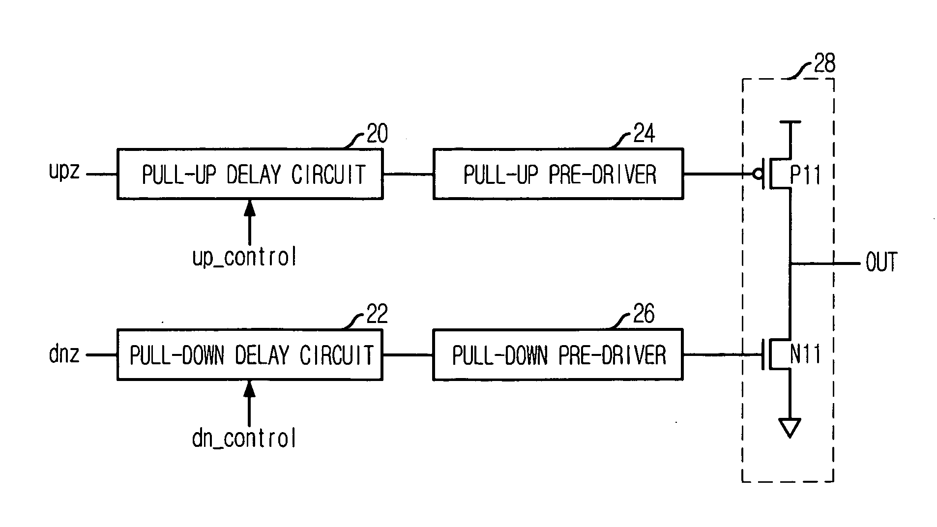
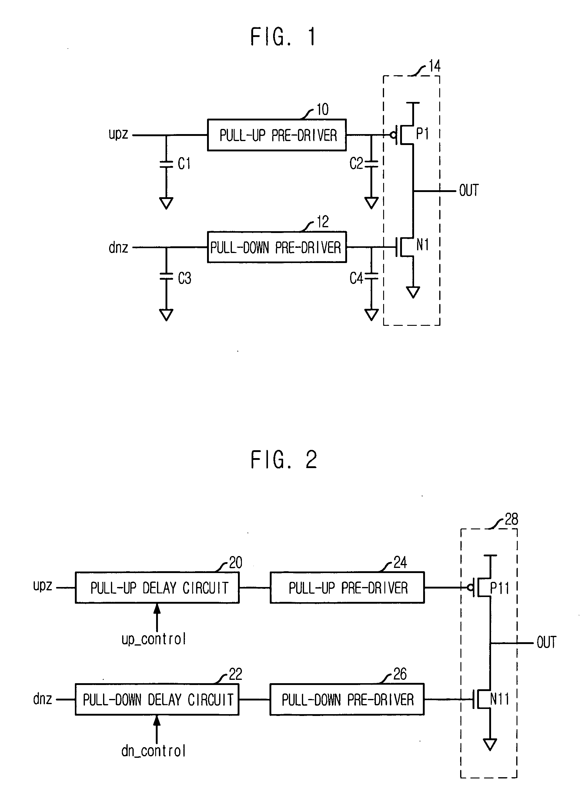
[0018]FIG. 2 is a circuit diagram of an output drive in accordance with one embodiment of the present invention.

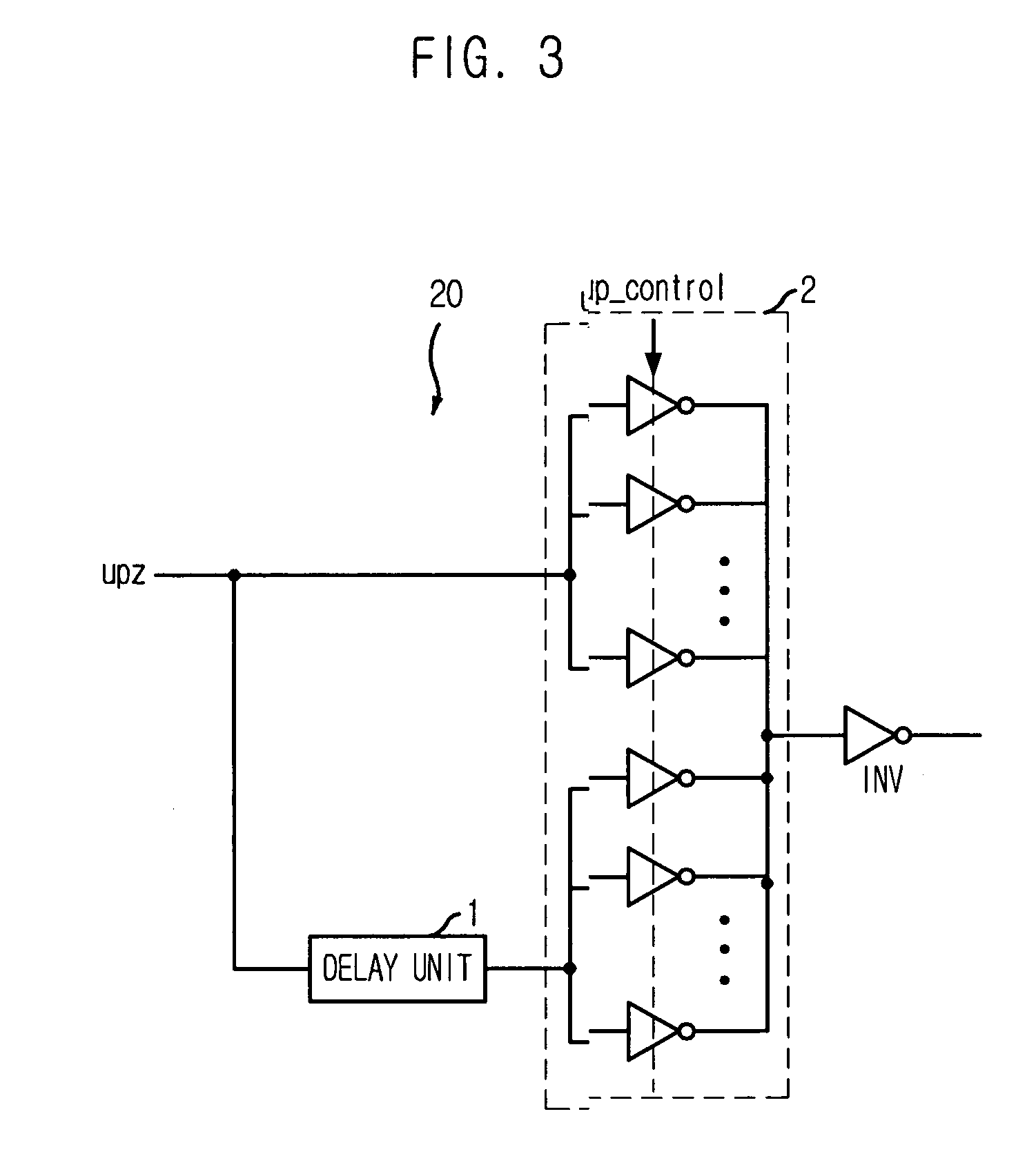
[0019] Referring to FIG. 2, the output driver of the present invention includes a main driver 28 having a pull-up PMOS transistor P11 and a pull-down NMOS transistor N11, a pull-up delay circuit 20 for controlling a delay time of a pull-up signal upz in response to a pull-up delay control signal up_control, a pull-down delay circuit 22 for controlling a delay time of a pull-down control signal dnz in response to a pull-down delay control signal dn_control, a pull-up pre-driver 24 for pre-driving a gate terminal of the pull-up PMOS transistor P11 in response to an output signal of the pull-up delay circuit 20, and a pull-down pre-driver 26 for pre-driving a gate terminal of the ...


PUM


Abstract

There is provided an output driver of a semiconductor device in which a slew rate variance is small despite an environmental change and a slew rate can be easily controlled. The output driver includes a main driver for driving an output terminal, a delay unit for controlling a delay time of a driving control signal in response to a delay control signal, and a pre-driver for pre-driving an input terminal of the main driver in response to an output signal of the delay unit.

Description

FIELD OF THE INVENTION [0001] The present invention relates to a design technology of a semiconductor circuit; and more particularly, to an output driver in a semiconductor device. DESCRIPTION OF RELATED ART [0002] A semiconductor memory device is fabricated based on various semiconductor technologies such as a processing technology of a silicon wafer and a logic design technology and so forth. A final product achieved through a semiconductor fabrication process is a plastic package typed chip, which retains a predetermined logic and function differentiated according to a purpose of use. Most of semiconductor chips are mounted on a printed circuit board, which is an important element for constituting a semiconductor system, and they need a predetermined driving voltage for operation. [0003] Whole the semiconductor devices including a semiconductor memory device are operated by input / output of signals of which each signal has its own specific purpose. That is, whether the semiconduct...

Claims


Application Information

Patent Timeline
Patent Type & Authority Applications(United States)
IPC IPC(8): H03K19/094
CPCH03K19/00384G11C7/1048G11C7/1063G11C7/22G11C29/023H03K21/10
Inventor NA, KWANG-JIN
Owner SK HYNIX INC
Features
  • R&D
  • Intellectual Property
  • Life Sciences
  • Materials
  • Tech Scout
  • Unparalleled Data Quality
  • Higher Quality Content
  • 60% Fewer Hallucinations
Learn More