Memory cell comprising one MOS transistor with an isolated body having a reinforced memory effect
- Summary
- Abstract
- Description
- Claims
- Application Information
AI Technical Summary
Benefits of technology
Problems solved by technology
Method used
Image

Examples
Embodiment Construction
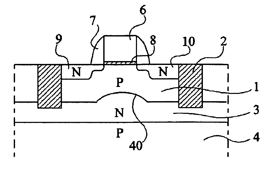
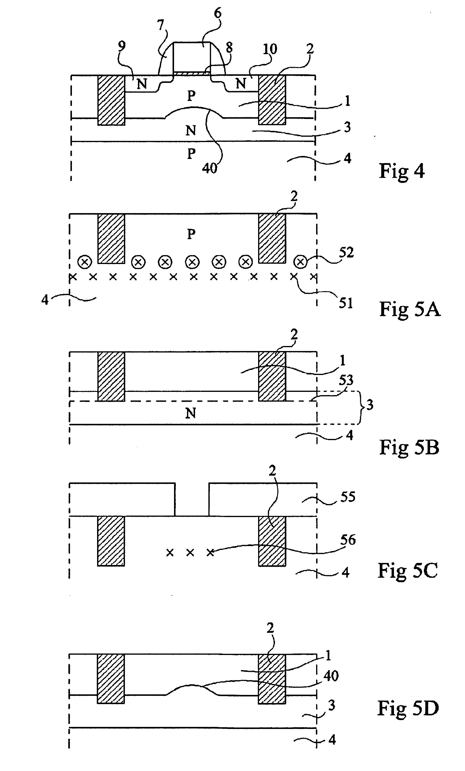
[0031] As usual in the representation of integrated circuits, the various cross-section views are not drawn to scale.
[0032]FIG. 4 shows, in a simplified cross-section view, an example of a memory cell with a transistor on a floating body according to an embodiment of the present invention. In this drawing, the same elements as in FIG. 1 are designated with the same reference numerals. In this cross-section view, no conductive area enabling creating a contact with buried layer 3, said contact being outside of the plane of the drawing or being common to a cell block, has been shown.
[0033] In this embodiment of the present invention, the junction surface between floating body 1 and buried layer 3 is non-planar. It exhibits a protrusion 40 substantially under the gate area of the MOS transistor. This results in increasing the junction surface with respect to the prior art case illustrated in FIG. 1 where the junction is planar.
[0034] The inventors have shown that such an increase in ...
PUM
 Abstract
Description
Claims
Application Information
 - Generate Ideas
- Intellectual Property
- Life Sciences
- Materials
- Tech Scout
- Unparalleled Data Quality
- Higher Quality Content
- 60% Fewer Hallucinations
Browse by: Latest US Patents, China's latest patents, Technical Efficacy Thesaurus, Application Domain, Technology Topic, Popular Technical Reports.
© 2025 PatSnap. All rights reserved.Legal|Privacy policy|Modern Slavery Act Transparency Statement|Sitemap|About US| Contact US: help@patsnap.com