Method and structure for reduction of soft error rates in integrated circuits

a technology of integrated circuits and soft errors, applied in the field of integrated circuits, can solve the problems of soft error rates in integrated circuits, upset the function of integrated circuits, and extra charge to reach

Active Publication Date: 2007-01-18
GLOBALFOUNDRIES US INC
View PDF2 Cites 35 Cited by
  • Summary
  • Abstract
  • Description
  • Claims
  • Application Information

AI Technical Summary

Benefits of technology

[0008] A fifth aspect of the present invention is the structure of the first aspect of the present invention, wherein the predetermined percentage of alpha particles is about 99% or greater of the alpha particles of the selected energy and wherein the selected energy is equal to or less than about 10 MeV.
[0009] A sixth aspect of the present invention is the structure of the first aspect of the present invention, wherein the metal wires comprise a structure selected from the group consisting of a damascene wire, a damascene via, a damascene terminal pad, a dual damascene wire having one or more integral vias, a dual damascene terminal pad having one or more integral vias and combinations thereof.
[0010] A seventh aspect of the present invention is the structure of the first aspect of the present invention, wherein the metal wires comprise material selected from the group consisting of Ta, TaN, Ti, TiN, W, WN, Ru, Cu and combinations thereof and the dielectric material is selected from the group consisting of silicon dioxide, fluorinated silicon dioxide, polyimide, a low K material having a permittivity of 4 or less, hydrogen silsesquioxane polymer, methyl silsesquioxane polymer, polyphenylene oligomer, SiOx(CH3)y, organosilicate glass, SiCOH, porous SiCOH, diamond-like carbon and combina...

Problems solved by technology

Soft error rates in integrated circuits are caused by ionizing radiation, such as alpha particles passing through the semiconductor materials of the integrated circuit.
Electric fields present in the integrated circuit can cause the holes and...

Method used


Image

  • Method and structure for reduction of soft error rates in integrated circuits
  • Method and structure for reduction of soft error rates in integrated circuits
  • Method and structure for reduction of soft error rates in integrated circuits

Examples


first embodiment

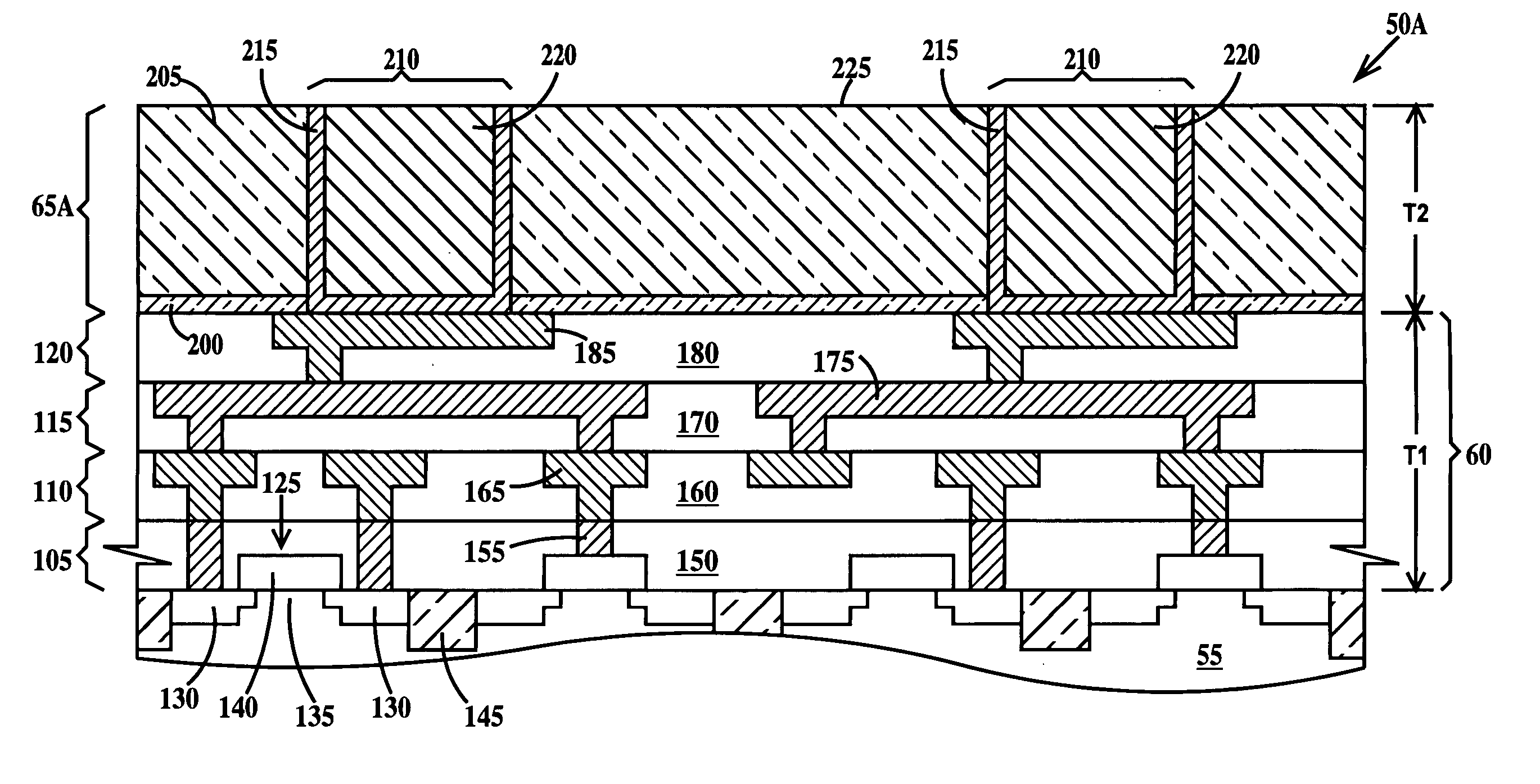
[0055]FIG. 3A is a top view and FIG. 3B is a cross-sectional view through line 3B-3B of FIG. 3A of an integrated circuit chip fabricated with a blocking layer according to the present invention. In FIG. 3B, an integrated circuit chip 50A includes substrate 55, wiring levels 60 and a blocking layer 65A. In a first example, substrate 55 may comprise a bulk silicon substrate. In a second example, substrate 55 may comprise a silicon-on-insulator (SOI) substrate. Wiring levels 60, having thickness T1, comprises individual wiring levels 105, 110, 115 and 120. Substrate 55 includes a multiplicity of field effect transistors (FETs) 125, each including source / drains 130 formed in substrate 55 and a channel region 135 formed in substrate 55 between source / drains 130 and under a gate electrode 140. There is also a gate dielectric layer (not shown) between gate electrode 140 and substrate 55.

[0056] Wiring level 105 includes a dielectric layer 150 in which damascene contacts 155 are formed. Wiri...

second embodiment

[0061]FIG. 4A is a top view and FIG. 4B is a cross-sectional view through line 4B-4B of FIG. 4A of an integrated circuit chip fabricated with a blocking layer according to the present invention. In FIG. 4B an integrated circuit chip 50B is similar to integrated circuit chip 50A of FIG. 3B except a damascene shield 230 comprising conductive liner 215 and core conductor 220 is formed in a blocking layer 65B and surrounds terminal pads 210 (see also FIG. 4A). Terminal pads 210 and shield 230 may be fabricated by the same damascene process or by separate damascene processes. Shield 230 is illustrated as not electrically connected to terminal pads 210 and not extending all the way through dielectric layers 200 and 205 to dielectric wiring level 120 or through dielectric layer 205 in the case that dielectric layer 200 is not present. Optionally, shield 230 may be connected to a terminal pad 210 in order to ground the shield or for other purposes.

third embodiment

[0062]FIG. 5A is a top view and FIG. 5B is a cross-sectional view through line5B-5B of FIG. 5A of an integrated circuit chip fabricated with a blocking layer according to the present invention. In FIG. 5B an integrated circuit chip 50C is similar to integrated circuit chip 50A of FIG. 3B except damascene dummy pads 235 comprising conductive liner 215 and core conductor 220 are formed in a blocking layer 65C between terminal pads 210 (see also FIG. 5A). Terminal pads 210 and dummy pads 235 may be fabricated by the same damascene process or by separate damascene processes. Dummy pads 235 are not electrically connected to terminal pads 210 and do not extend all the way through dielectric layers 200 and 205 to dielectric wiring level 120 or through dielectric layer 205 in the case that dielectric layer 200 is not present. Dummy pads 235 serve to increase the uniformity of the CMP process used to form the blocking layer 65C.


PUM


Abstract

A structure and a method for reduction of soft error rates in integrated circuits. The structure including: a semiconductor substrate; and a stack of one or more wiring levels stacked from a lowermost wiring level to an uppermost wiring level, the lowermost wiring level nearer the semiconductor substrate than the uppermost wiring level; and an alpha particle blocking layer on a top surface of the uppermost wiring level of the one or more wiring levels, the blocking layer comprising metal wires and a dielectric material, the blocking layer having a combination of a thickness of the blocking layer and a volume percent of metal wires in the blocking layer sufficient to stop a predetermined percentage of alpha particles of a selected energy or less striking the blocking layer from penetrating into the stack of one or more wiring levels or the substrate.

Description

FIELD OF THE INVENTION [0001] The present invention relates to the field of integrated circuits; more specifically, it relates to a method and a structure for the reduction of soft error rates in integrated circuits. BACKGROUND OF THE INVENTION [0002] Soft error rates in integrated circuits are caused by ionizing radiation, such as alpha particles passing through the semiconductor materials of the integrated circuit. Both logic and memory circuits may be effected. The errors are called “soft” because they generally only persist until the next cycle of the integrated circuit function. As an alpha particle passes through semiconductor material a “cloud” of hole-electron pairs are generated in the vicinity of its path. Electric fields present in the integrated circuit can cause the holes and electrons to migrate in opposite directions thus causing extra charge to reach particular circuit nodes and upset the function of the integrated circuit. [0003] As integrated circuit devices contin...

Claims


Application Information

Patent Timeline
IPC IPC(8): H01L23/52H01L23/48H01L29/40
CPCH01L21/76801H01L21/76834H01L21/76838H01L23/5329H01L23/53295H01L23/556H01L23/585H01L24/03H01L24/05H01L24/12H01L24/16H01L24/48H01L2224/0401H01L2224/04042H01L2224/05006H01L2224/05572H01L2224/05599H01L2224/13007H01L2224/13022H01L2224/131H01L2224/13111H01L2224/16H01L2224/48227H01L2224/48465H01L2224/85399H01L2924/01002H01L2924/01005H01L2924/01007H01L2924/01013H01L2924/01014H01L2924/01015H01L2924/0102H01L2924/01022H01L2924/01027H01L2924/01028H01L2924/01029H01L2924/01033H01L2924/01046H01L2924/01047H01L2924/0105H01L2924/01057H01L2924/01063H01L2924/01073H01L2924/01074H01L2924/01078H01L2924/01082H01L2924/01092H01L2924/014H01L2924/04941H01L2924/04953H01L2924/05042H01L2924/14H01L2924/15174H01L2924/15312H01L2924/19041H01L2924/19042H01L2924/19043H01L2924/30107H01L2924/3025H01L2924/00014H01L2924/01006H01L2924/01019H01L2924/01024H01L2924/01044H01L2924/01055H01L2924/01084H01L2224/451H01L2924/10253H01L2224/05554H01L2924/1306H01L2924/1305H01L2924/0002H01L2224/45099H01L2924/00H01L2224/05552H01L2924/15787H01L24/45H01L21/28H01L23/48H01L21/3205
Inventor CABRAL, CYRIL JR.GORDON, MICHAEL S.RODBELL, KENNETH P.
Owner GLOBALFOUNDRIES US INC
Why Eureka
Try Eureka