
Resonator, filter, and communication unit

a filter and communication unit technology, applied in the direction of waveguide devices, resonators, basic electric elements, etc., can solve the problems of difficult to obtain a predetermined resonant frequency with high precision, and the line width cannot be extremely narrow, so as to achieve the effect of small communication apparatus and size of high-frequency circuit parts

Active Publication Date: 2007-01-18
MURATA MFG CO LTD
View PDF8 Cites 2 Cited by
  • Summary
  • Abstract
  • Description
  • Claims
  • Application Information

AI Technical Summary

Benefits of technology

[0012] According to this invention, a communication apparatus including the above-described resonator or filter is provided. By the provision of this filter, the size of a high-frequency circuit portion including the above-described resonator or filter can be reduced, thereby obtaining a small communication apparatus.

Problems solved by technology

However, because of a restriction on the pattern forming precision of the conductive film, the line width cannot be formed to be extremely narrow.
Thus, it is more difficult to obtain a predetermined resonant frequency with high precision as the line width of the conductor opening APc in the capacitive area becomes narrower.

Method used


Image

  • Resonator, filter, and communication unit
  • Resonator, filter, and communication unit
  • Resonator, filter, and communication unit

Examples


first embodiment

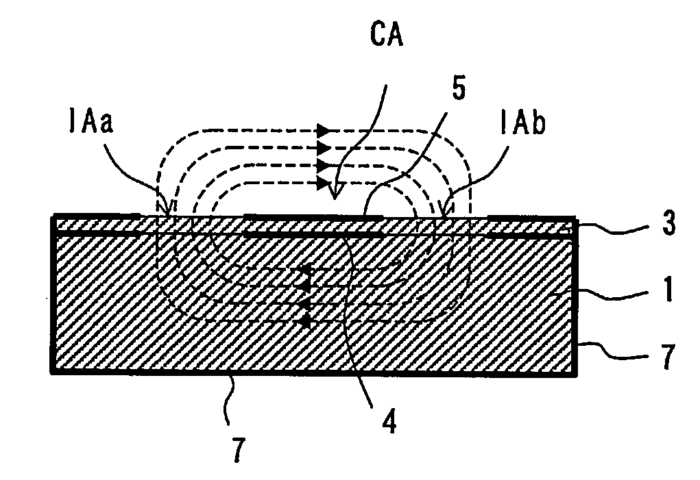
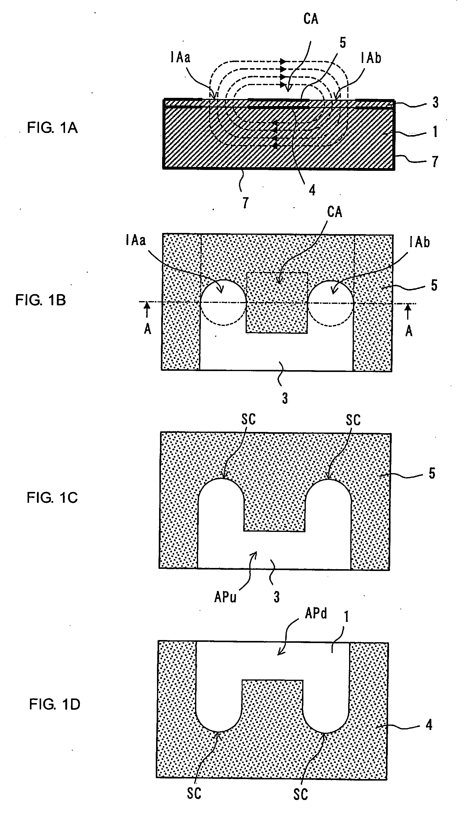
[0015] A resonator is discussed below with reference to FIG. 1.

[0016] In FIG. 1, (B) is a top view illustrating the resonator, (A) is a sectional view taken along line A-A in (B), (C) illustrates the pattern of a conductor layer disposed on the top surface, and (D) illustrates the pattern of a conductor layer pattern disposed as the bottom layer.

[0017] On the top surface of a rectangular dielectric substrate 1, a conductor layer 4 having the pattern shown in (D) is formed. A dielectric layer 3 is disposed on the entire top surface of the dielectric substrate 1 on which the conductor layer 4 is formed, and a conductor layer 5 having the pattern shown in (C) is formed on the surface of the dielectric layer 3. With this configuration, a structure in which the conductor layers 4 and 5 are laminated in the thickness direction with the dielectric layer 3 therebetween is formed. In the state in which the conductor layers 4 and 5 are laminated with the dielectric layer 3 therebetween, con...

second embodiment

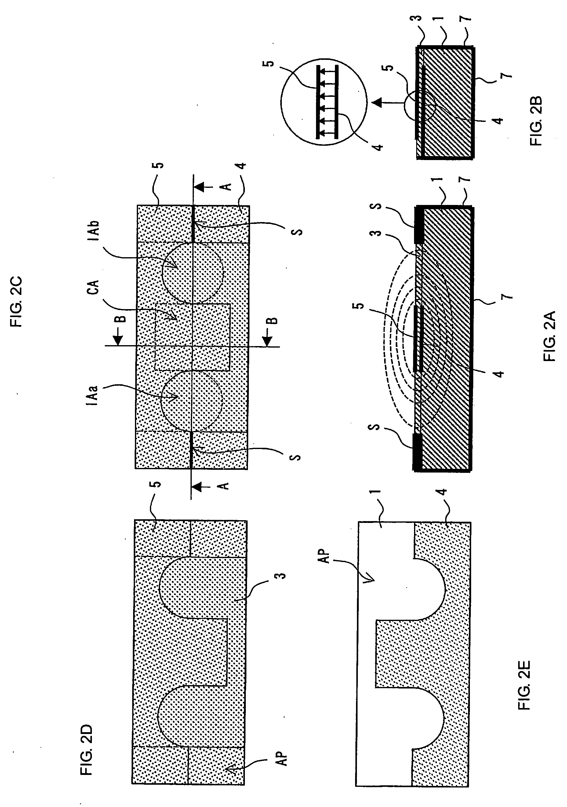
[0026]FIG. 2 illustrates the configuration of a resonator according to a In FIG. 2, (C) is a top view illustrating the resonator, (A) is a sectional view taken along line A-A in (C), and (B) is a sectional view taken along line B-B in (C). In FIG. 2, (D) illustrates the pattern of a conductor layer 5 as the upper layer, and (E) illustrates the pattern of a conductor layer 4 as the lower layer. Unlike the resonator shown in FIG. 1, in this resonator shown in FIG. 2, the conductor layers 4 and 5 are partially electrically connected to each other by interlayer short-circuit portions S on the top surface of the dielectric substrate 1. The dielectric layer 3 is not present in the interlayer short-circuit portions S. According to this structure, the conductor layers 4 and 5 are short-circuited more reliably in the vicinities of the conductor openings by the interlayer short-circuit portions S compared to the structure in which the conductor layers 4 and 5 are short-circuited only by the ...

third embodiment

[0027]FIG. 3 illustrates the configuration of a resonator according to a In FIG. 3, (C) is a top view illustrating the resonator, (A) is a sectional view taken along line A-A in (C), and (B) is a sectional view taken along line B-B in (C). In FIG. 3, (D) illustrates the pattern of a conducive layer 5 as the upper layer, and (E) illustrates the pattern of a conductor layer 6 as the lower layer.

[0028] The conductor layer 6 is formed in a predetermined portion on the top surface of the dielectric substrate 1. The conductor layer 5 having the pattern shown in (D) is formed on the top surface of the conductor layer 6 with the dielectric layer 3 therebetween. The conductor opening of the conductor layer 5 is formed in a dumbbell shape in which generally circular conductor openings APa and APb are formed at both ends and a slot conductor opening APc having a predetermined width is interposed between the conductor openings APa and APb. The conductor layer 6 is formed in a position near the...


PUM


Abstract

A resonator, a filter, and a communication apparatus that can be easily miniaturized even if the resonant frequency is relatively low are provided. Conductor layers are laminated in the state in which they are partially insulated from each other by a dielectric layer. Conductor openings free from any conductor layer in the laminate direction serve as inductive areas, and the portion where the conductor layers oppose each other with the dielectric layer therebetween serves as a capacitive area CA. With this configuration, the resulting resonator serves as a stepped-impedance-structured slot resonator. By increasing the impedance step ratio of the capacitive area to the inductive areas according to this structure, the resonator is miniaturized. Additionally, the conductor loss of the resonator is reduced by suppressing the intrusion of magnetic field energy to the capacitive area. It is thus possible to obtain a small resonator having high Qo.

Description

TECHNICAL FIELD [0001] The present invention relates to a resonator, a filter, and a communication apparatus which are used, for example, for wireless communication in microwaves or millimeter waves or for sending and receiving electromagnetic waves. BACKGROUND ART [0002] Hitherto, to reduce the size of a resonator using a slot line, a design approach to form the slot line into a stepped impedance structure is known (for example, see “ANALYSIS, DESIGN AND APPLICATIONS OF FIN LINES”, Bharathi Bhat, Shiban K. Koul, PP. 316-17 published by ARTECH HOUSE, INC, U.S.A. 1987, and “MAIKUROHA KAIRO NO KISO TO OHYO (BASICS AND APPLICATIONS OF MICROWAVE CIRCUITS), Yoshihiro KONISHI, Sougou Denshi Shuppannsha, p. 169 issued in 1990 (first edition). In this approach, by forming the widths of both ends of the slot line to be larger and by forming the width of the central portion to be narrower, the impedance of both ends of the slot line becomes inductive and the impedance of the central portion b...

Claims


Application Information

Patent Timeline
IPC IPC(8): H01P1/20H01P7/04H01P1/201H01P7/08
CPCH01P7/082H01P1/2016
Inventor HIDAKA, SEIJIABE, SHIN
Owner MURATA MFG CO LTD
Learn More