Liquid crystal display device

a liquid crystal display and display device technology, applied in non-linear optics, instruments, optics, etc., can solve the problems of lowering the display quality of the liquid crystal display device, different directions, and t-v characteristics obtained, and achieve superior display quality and high luminance.

Inactive Publication Date: 2007-01-25
SHARP KK
View PDF13 Cites 34 Cited by
  • Summary
  • Abstract
  • Description
  • Claims
  • Application Information

AI Technical Summary

Benefits of technology

[0022] The invention can realize a liquid crystal display device which is high in luminance and superior in display quality.

Problems solved by technology

However, VA (vertically aligned)-mode liquid crystal display devices, for example, have a problem that a transmittance vs. application voltage characteristic (T-V characteristic) obtained when the display screen is viewed from the direction perpendicular to it (i.e., front direction) is different from that obtained when the display screen is viewed from a oblique direction.
Liquid crystal display devices of the TN (twisted nematic) mode, which is a more conventional drive mode, have the same problem.
However, the liquid crystal display device shown in FIG. 14 has the following problems.
This results in a problem that the display quality of the liquid crystal display device is much lowered.
However, if the end portions of the pixel electrodes 116 and 117 are set away from the drain bus line 114, the region where the pixel electrodes 116 and 117 are formed is made narrow, resulting in a problem that the pixel aperture ratio and the luminance decrease.
Further, a prescribed bonding registration error occurs when the TFT substrate and the counter substrate are bonded to each other.
This results in a problem that the pixel aperture ratio and the luminance decrease further.

Method used


Image

  • Liquid crystal display device
  • Liquid crystal display device
  • Liquid crystal display device

Examples


first embodiment

[First Embodiment]

[0039] A liquid crystal display device according to a first embodiment of the present invention will be described below with reference to FIGS. 1-6.

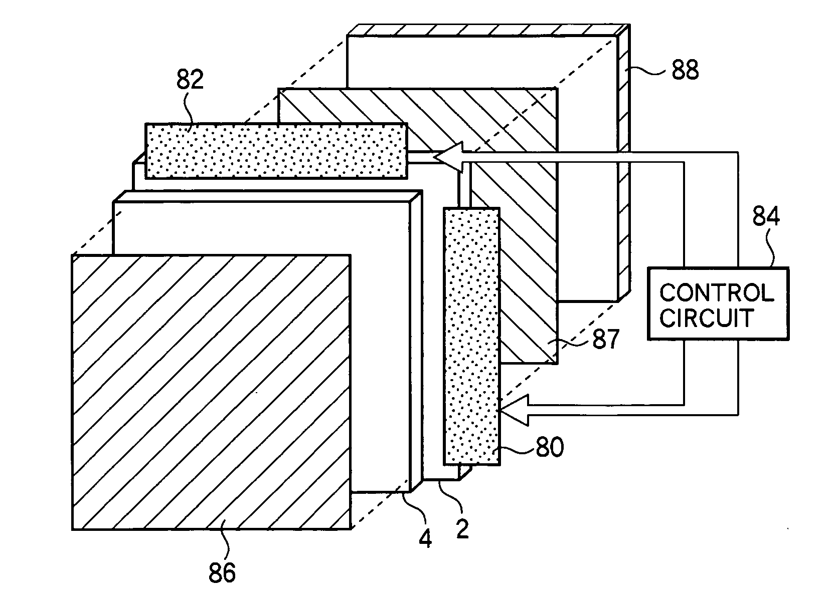
[0040]FIG. 1 schematically shows the configuration of the liquid crystal display device according to this embodiment. As shown in FIG. 1, the liquid crystal display device has a TFT substrate 2 which is provided with gate bus lines and drain bus lines that cross each other with an insulating film interposed in between, TFTs which are formed for the respective pixels, and pixel electrodes. The liquid crystal display device is also equipped with a counter substrate 4 opposed to the TFT substrate 2, in which color filters and a common electrode are formed and a liquid crystal 6 (not shown in FIG. 1) which is sealed between the substrates 2 and 4 and has negative dielectric anisotropy, for example. Vertical alignment films (not shown) for aligning the liquid crystal 6 vertically are formed at the boundary between the liqui...

second embodiment

[Second Embodiment]

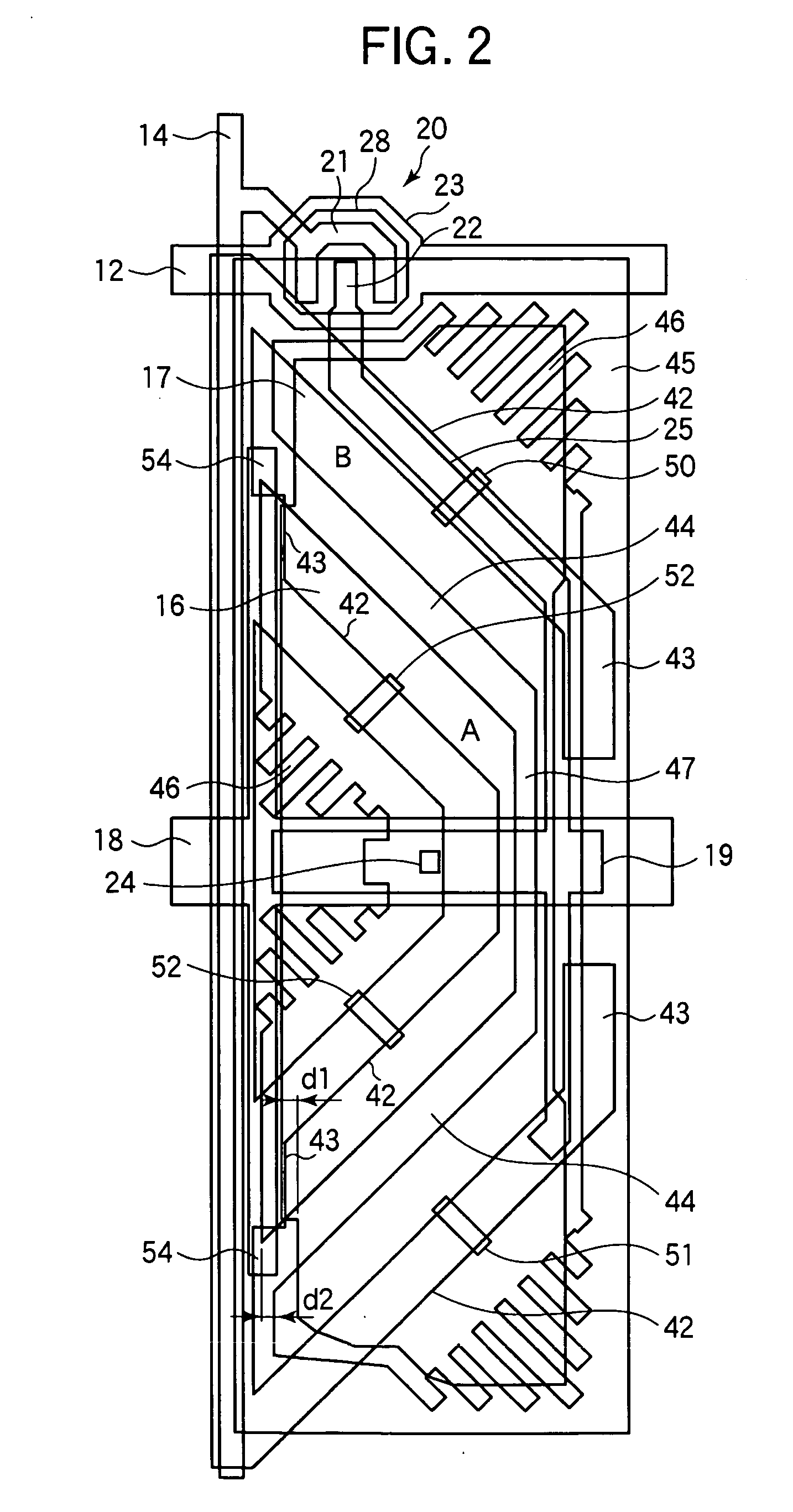
[0061] Next, a liquid crystal display device according to a second embodiment of the invention will be described with reference to FIG. 7. FIG. 7 shows a one-pixel configuration of the liquid crystal display device according to this embodiment. As shown in FIG. 7, this embodiment is different from the first embodiment in that four apertures 52 are disposed in the top portion and the bottom portion of the pixel region (two apertures 52 in each portion) so as to be approximately line-symmetrical with respect to the storage capacitor bus line 18. Two apertures 52 are disposed close to both ends, in the longitudinal direction, of the overlap region, as viewed perpendicularly to the substrate surfaces, of the associated linear projection 42 and the pixel electrode 16. As a result, in the sub-pixel A, singular points (s=−1) are formed in the regions of formation of the two apertures 52 that are close to both ends of the overlap region of the associated linear projection...

third embodiment

[Third Embodiment]

[0063] Next, a liquid crystal display device according to a third embodiment of the invention will be described with reference to FIG. 8. FIG. 8 shows a one-pixel configuration of the liquid crystal display device according to this embodiment. As shown in FIG. 8, the apertures 50, 51, and 52 are disposed in the same manner as in the first embodiment. This embodiment is different from the first embodiment in that that portion of the control capacitance electrode 25 which is located in the top portion of the sub-pixel B has a bypass portion 25a which bypasses the region of formation of the aperture 50 in the plane parallel with the substrate surfaces. With this measure, the aperture 50 does not overlap with the control capacitance electrode 25 and hence no electrode exists on the TFT substrate 2 side in the region of formation of the aperture 50. Therefore, a singular point (s=−1) is formed in the region of formation of the aperture 50 as in the regions of formation ...


PUM

PropertyMeasurementUnit
thickaaaaaaaaaa
angleaaaaaaaaaa
heightaaaaaaaaaa

Abstract

A liquid crystal display device includes a pair of substrates; a liquid crystal sealed between the substrates; plural pixel regions each having a first pixel electrode formed on one of the pair of substrates and a second pixel electrode separated from the first pixel electrode; a TFT having a source electrode which is electrically connected to the first pixel electrode; a control capacitance portion which has a control capacitance electrode electrically connected to the source electrode and opposed to at least part of the second pixel electrode via an insulating film, and which thereby establishes capacitive coupling between the source electrode and the second pixel electrode; linear projections formed on the other substrate; and apertures formed in the first and second pixel electrodes so as to occupy parts of overlap regions of the linear projections and the first and second pixel electrodes as viewed perpendicularly to the substrate surfaces, for controlling the positions of singular points of alignment vectors of the liquid crystal.

Description

BACKGROUND OF THE INVENTION [0001] 1. Field of the Invention [0002] The present invention relates to a liquid crystal display device used as, for example, a display unit of an electronic apparatus. [0003] 2. Description of the Related Art [0004] In recent years, liquid crystal display devices have come to be used for TV sets, monitor devices of personal computers, etc. In these purposes, liquid crystal display devices are required to have a superior viewing angle characteristic that the display screen is viewable from all directions. [0005] However, VA (vertically aligned)-mode liquid crystal display devices, for example, have a problem that a transmittance vs. application voltage characteristic (T-V characteristic) obtained when the display screen is viewed from the direction perpendicular to it (i.e., front direction) is different from that obtained when the display screen is viewed from a oblique direction. More specifically, the color of an image on the display screen looks more...

Claims


Application Information

Patent Timeline
Patent Type & Authority Applications(United States)
IPC IPC(8): G02F1/1343
CPCG02F1/133707G02F1/1393G02F1/133753
Inventor TASAKA, YASUTOSHISHIBASAKI, MASAKAZUNAKANISHI, YOHEIYOSHIDA, HIDEFUMIKAMADA, TSUYOSHIUEDA, KAZUYATSUDA, HIDEAKI
Owner SHARP KK
Why Eureka
Try Eureka