Methods of fabricating silicon carbide crystals

a technology of silicon carbide crystals and silicon carbide wafers, which is applied in the direction of single crystal growth, polycrystalline material growth, chemistry apparatus and processes, etc., can solve the problems of reducing the suitability of silicon carbide regions, micropipes or other defects in silicon carbide, and dislocation defects

Inactive Publication Date: 2007-02-01
CREE INC
View PDF48 Cites 11 Cited by
  • Summary
  • Abstract
  • Description
  • Claims
  • Application Information

AI Technical Summary

Problems solved by technology

One difficulty with silicon carbide is that silicon carbide may contain micropipes or other defects, such as dislocation defects.
Such defects may reduce the suitability of regions of a silicon carbide wafer containing such defects for use in a semiconductor device.
However, growth of silicon carbide crystals (e.g. boules) suitable for providing wafers or substrates is typically not carried out using CVD processes but is performed using physical vapor transport (PVT) growth, such as through a sublimation growth process as described above.

Method used


Image

  • Methods of fabricating silicon carbide crystals
  • Methods of fabricating silicon carbide crystals
  • Methods of fabricating silicon carbide crystals

Examples


Embodiment Construction

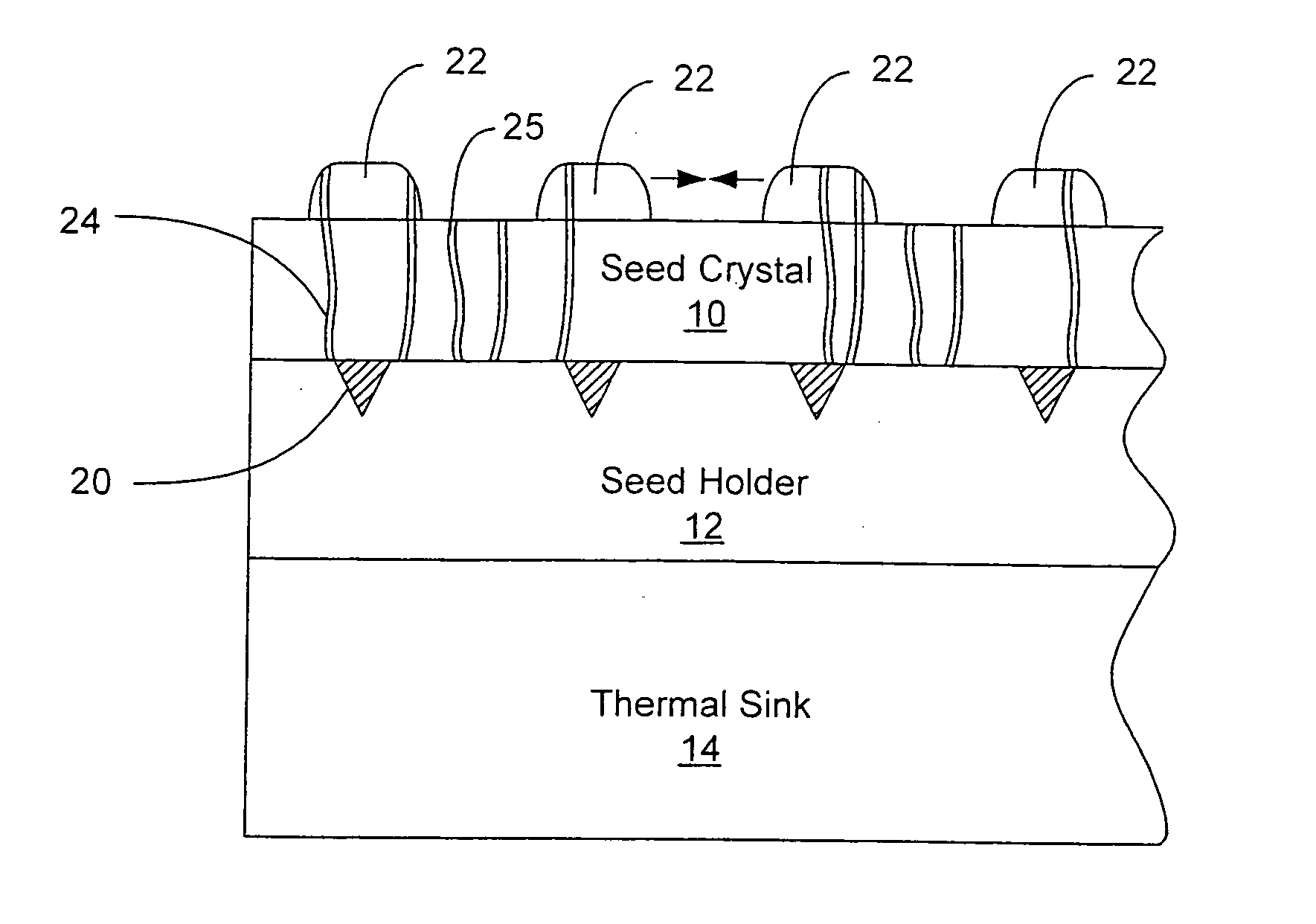
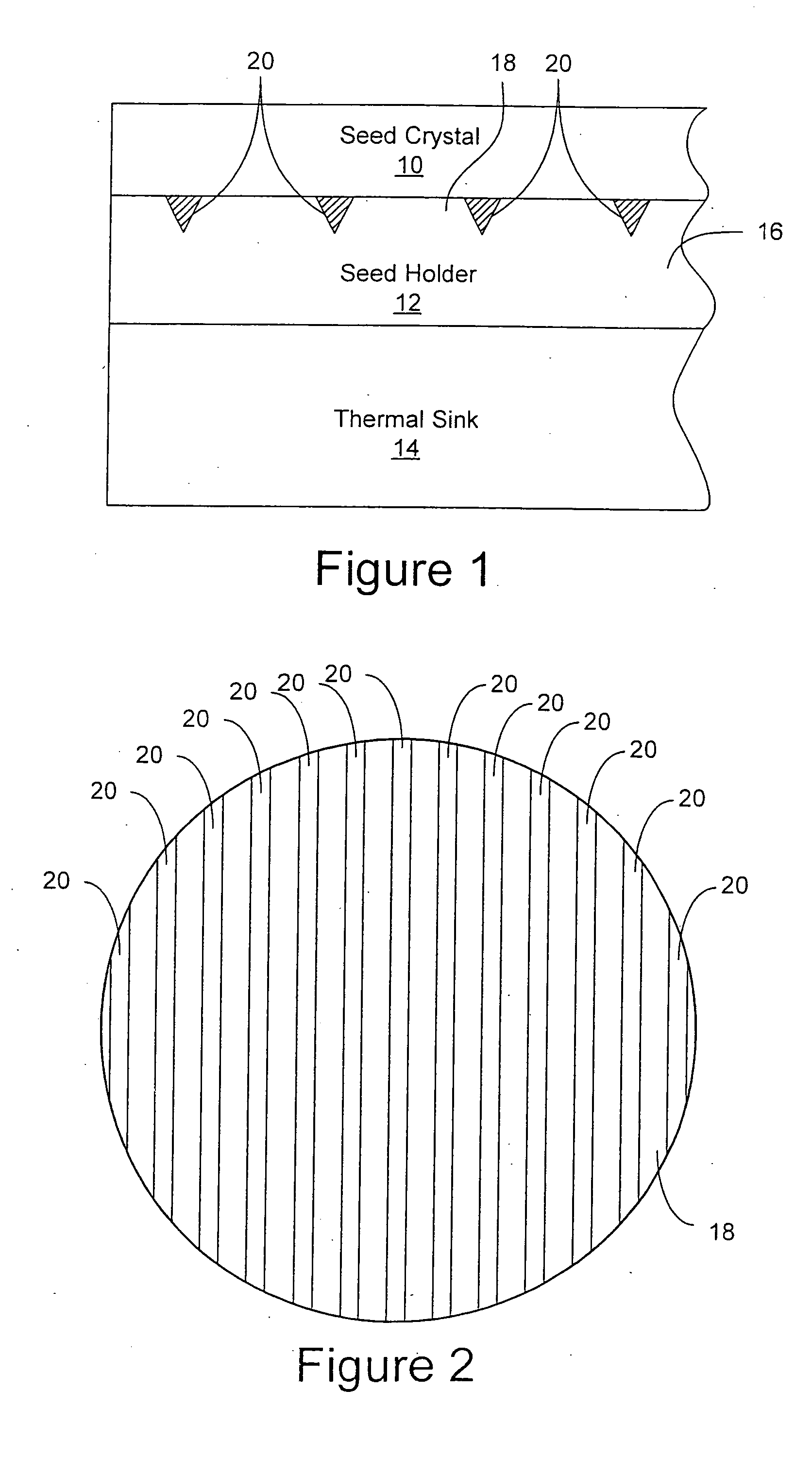
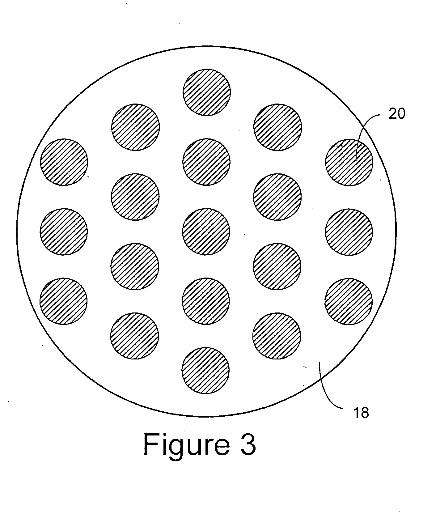
[0027] The present invention now will be described more fully hereinafter with reference to the accompanying drawings, in which preferred embodiments of the invention are shown. This invention may, however, be embodied in many different forms and should not be construed as limited to the embodiments set forth herein; rather, these embodiments are provided so that this disclosure will be thorough and complete, and will fully convey the scope of the invention to those skilled in the art. In the drawings, the thickness of layers and regions are exaggerated for clarity. Like numbers refer to like elements throughout. It will be understood that when an element such as a layer, region or substrate is referred to as being “on” another element, it can be directly on the other element or intervening elements may also be present. In contrast, when an element is referred to as being “directly on” another element, there are no intervening elements present.

[0028] Embodiments of the present inve...


PUM

PropertyMeasurementUnit
widthaaaaaaaaaa
depthaaaaaaaaaa
widthaaaaaaaaaa

Abstract

Methods for producing silicon carbide crystals, seed crystal holders and seed crystal for use in producing silicon carbide crystals and silicon carbide crystals are provided. Silicon carbide crystals are produced by forcing nucleation sites of a silicon carbide seed crystal to a predefined pattern and growing silicon carbide utilizing physical vapor transport (PVT) so as to provide selective preferential growth of silicon carbide corresponding to the predefined pattern. Seed holders and seed crystals are provided for such methods. Silicon carbide crystals having regions of higher and lower defect density are also provided.

Description

RELATED APPLICATIONS [0001] The present application is a continuation of and claims priority from U.S. patent application Ser. No. 10 / 756,542, filed Jan. 13, 2004, which is a continuation of U.S. patent application Ser. No. 09 / 862,108, filed May 21, 2001 entitled Seed Crystal Holders and Seed Crystals for Fabricating Silicon Carbide Crystals and Methods of Fabricating Silicon Carbide Crystals (now U.S. Pat. No. 6,706,114), the disclosures of which are incorporated herein as if set forth fully herein.FIELD OF THE INVENTION [0002] The present invention relates to the fabrication of semiconductor materials and, more particularly, to devices for use in fabricating silicon carbide crystals and the fabrication of silicon carbide crystals, for example, to produce silicon carbide boules from which a silicon carbide wafer may be provided. BACKGROUND OF THE INVENTION [0003] Silicon carbide (SiC) is rarely found in nature. It has, however, been manufactured for more than eighty years, in cryst...

Claims


Application Information

Patent Timeline
Patent Type & Authority Applications(United States)
IPC IPC(8): C30B23/00C30B25/00C30B28/12C30B28/14
CPCC30B23/00C30B23/025Y10S117/911C30B29/36
Inventor MUELLER, STEPHAN
Owner CREE INC
Why Eureka
Try Eureka