Seamless stitching of patterns formed by interference lithography

a technology of interference lithography and pattern stitching, applied in photographic processes, radiation therapy, therapy, etc., can solve the problems of limited use of coherent pattern sizes, practical limitations, and barriers to commercial application of these nanotechnologies, and achieve the effect of high-speed optical modulation

Active Publication Date: 2007-02-01
VINCENT E STENGER
View PDF19 Cites 28 Cited by
  • Summary
  • Abstract
  • Description
  • Claims
  • Application Information

AI Technical Summary

Benefits of technology

[0009] This patent disclosure describes several approaches to implementation of optical feedback and positioning for stitch alignment of nanometer and micrometer scale patterns formed by methods such as interference lithography. Due to the regularity and periodicity of the step-and-repeat tiled patterns at their boundaries, adjacent exposures can be stitch aligned by observing the pattern optical transmissions, or other suitable signals, in the pattern overlap regions. In this fashion, each new exposure is locked onto a previous exposure. Such stitch tiling can be extended to cover arbitrarily large areas with a smaller base pattern. In an

Problems solved by technology

The issue now is that useful coherent pattern sizes are typically limited to a few inches, creating a barrier to commercial application of these nanotechnologies.
However, this has practical limitations, as larger distances will incur more pointing and vibration sensitivity, as well as wave front phase randomization, all of which will tend to wash out the developed exposure pattern.
The other issue is that the exposure intensity is reduced rapidly in a square law sense as the distance is increased, leading to increased exposure times. As an example, an increase in diameter coverage by a factor two incurs an exposure time increase of a factor four.
This is due mostly to discontinuous phase boundaries and stitch related defects.
Due to practical tolerance issues, such mechanical tiling inherently results in large stitching errors in all 3 dimensions (x, y, and z) when applied to micro and nanometer scale textures.
At best, such errors would result in cosmetic an

Method used


Image

  • Seamless stitching of patterns formed by interference lithography
  • Seamless stitching of patterns formed by interference lithography
  • Seamless stitching of patterns formed by interference lithography

Examples


Embodiment Construction

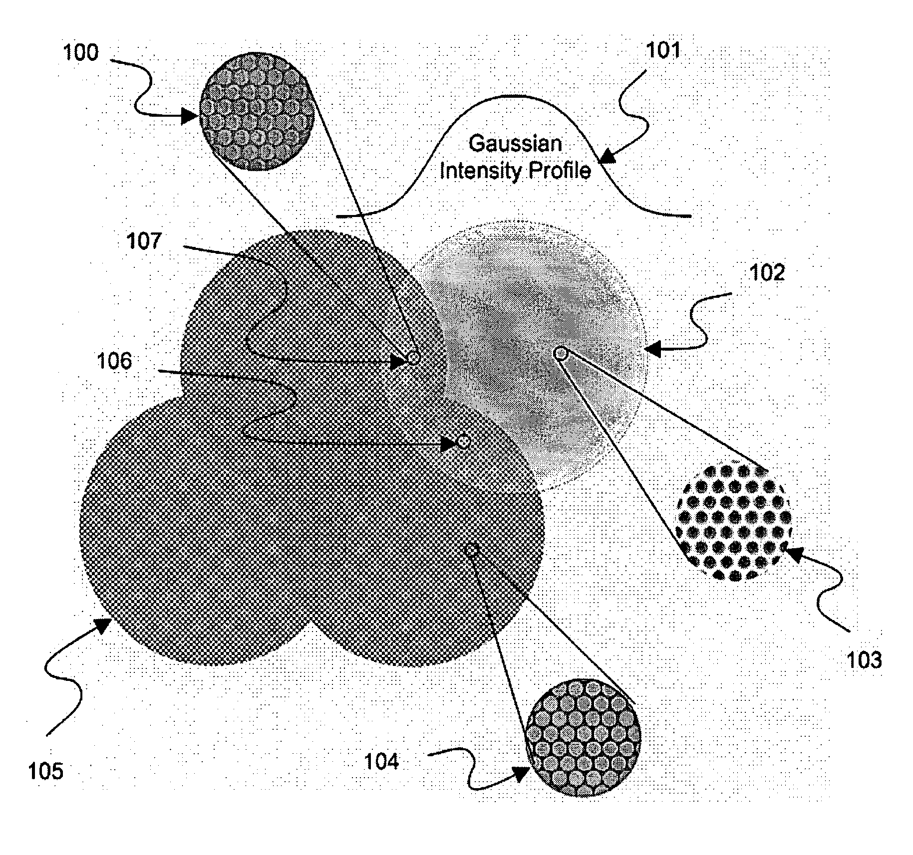
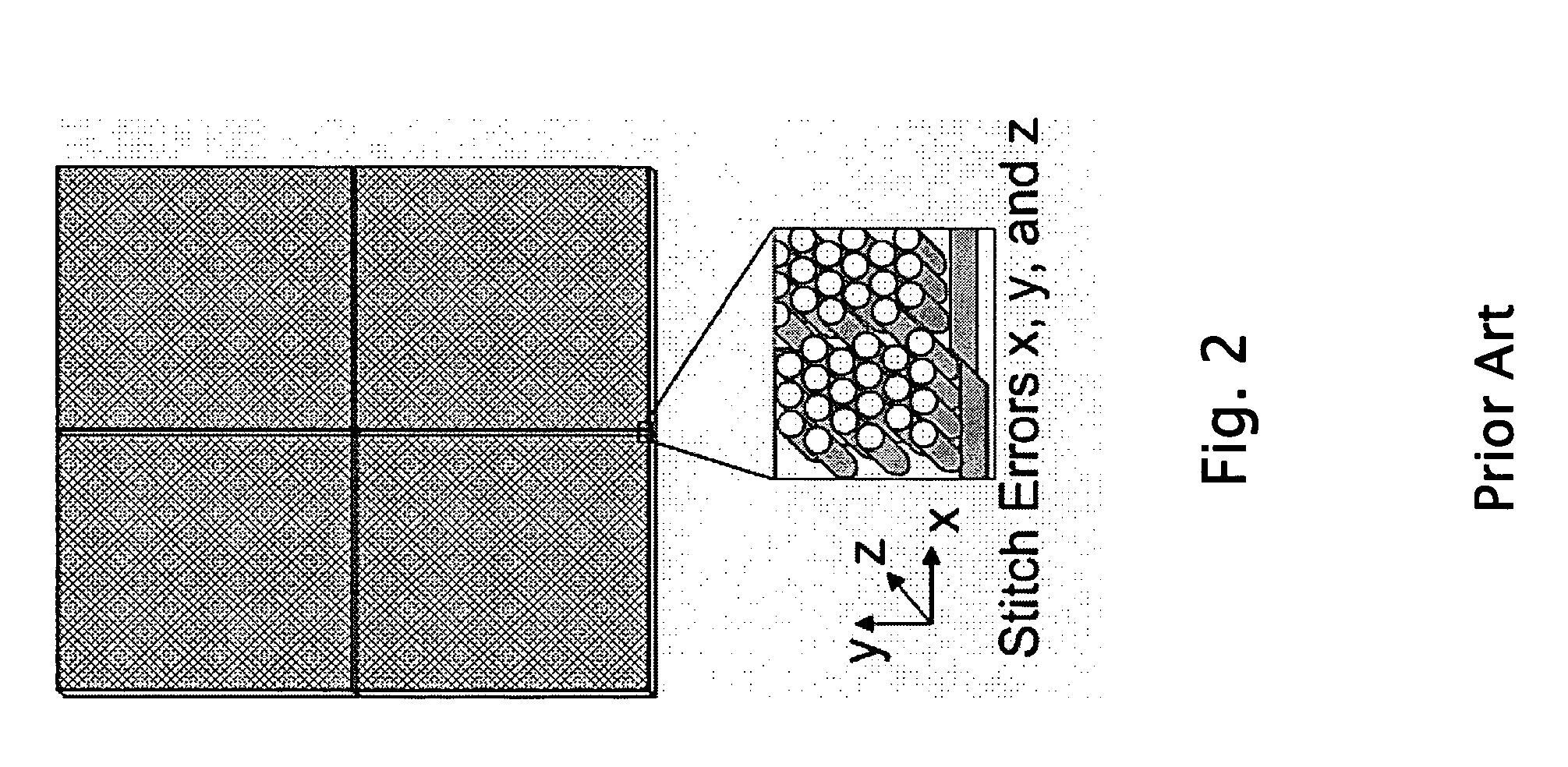
[0025] The current invention pertains to a novel, simple, and cost effective method to seamlessly tile and stitch regular surface textures, such as those with periodic nanometer scale features, at the exposure level of the fabrication process. An example of exposure level tile stitching of patterns in accordance with an exemplary embodiment of the present invention is shown in FIG. 4. Exposure pattern 102 may be generated by any of a number of ways, such as through interference by a plurality of monochromatic beams. Post exposures 105 represent impression of base pattern 102 at a plurality of partially overlapping tiled positions. The impression is manifested in the form of a transmission mask, or some other permanent or semi-permanent effect in the surface being exposed that can be used to register the post exposure pattern fine position relative to the new exposure pattern 102 position. Corresponding zoom view details are shown for base pattern 103 and for post-exposures 104, and ...


PUM


Abstract

This invention addresses the scalability problem of periodic “nanostructured” surface treatments such as those formed by interference lithography. A novel but simple method is described that achieves seamless stitching of nanostructure surface textures at the pattern exposure level. The described tiling approach will enable scaling up of coherent nanostructured surfaces to arbitrary area sizes. Such a large form factor nanotechnology will be essential for fabricating large aperture, coherent diffractive elements. Other applications include high performance, antiglare/antireflection and smudge resistant Motheye treatments for display products such as PDA's, laptop computers, large screen TV's, cockpit canopies, instrument panels, missile and targeting domes, and, more recently, “negative-index” surfaces. Although ideal for seamless stitching of nanometer scale patterns, the technology is broadly applicable to any situation where an arbitrarily large area needs to be seamlessly tiled with a smaller base pattern that has periodic overlap able boundaries.

Description

[0001] This application claims the benefit of provisional patent application No. 60 / 691,158 file date Jun. 17, 2005TECHNICAL FIELD OF THE INVENTION [0002] This invention pertains directly to the field of interference lithography and nanotechnology. However, the invention can be applied to any situation where a large area needs to be seamlessly tiled with a smaller base pattern by any of a multitude of pattern exposure or impression mechanisms. BACKGROUND OF THE INVENTION [0003] Nano structured and micro structured surfaces have been investigated for many years in terms of the special functional properties that can be achieved. For example, surfaces made up of many small “protuberances”, such as closely and regularly spaced cones, at the micron or sub-micron scale, can exhibit self-cleaning as well as near omni-directional and polarization insensitive anti-reflective properties at optical wavelengths. When features are on the nanometer scale, such so-called “Motheye” nanotextured sur...

Claims


Application Information

Patent Timeline
IPC IPC(8): A61N5/00
CPCG03F7/70408G03F9/7088G03F9/7011G03F7/70475
Inventor STENGER, VINCENT E.
Owner VINCENT E STENGER
Why Eureka
Try Eureka