Silicon semiconductor based high-speed ring optical modulator

a silicon semiconductor and ring optical technology, applied in the direction of optical waveguide light guide, instruments, optics, etc., can solve the problems of complex packaging of compound semiconductor optical devices and silicon semiconductor chips, the signal communication speed between semiconductor chips has not increased accordingly, and the high-speed compound semiconductor optical device is still relatively expensive. achieve the effect of reducing the size of the optical device, high speed, and improving the confinement ratio

Inactive Publication Date: 2010-01-12
ELECTRONICS & TELECOMM RES INST
View PDF9 Cites 2 Cited by
  • Summary
  • Abstract
  • Description
  • Claims
  • Application Information

AI Technical Summary

Benefits of technology

[0030]The high speed ring optical modulator according to the present invention uses a bipolar transistor in the variation portion of the refractive index, and thus carriers can be supplied and discharged at high speed, and the confinement ratio is improved to reduce the size of the optical device and high speed optical modulation is enabled also by supplying a small electric current.

Problems solved by technology

However, despite this, the signal communication speed between semiconductor chips has not increased accordingly.
However, high-speed compound semiconductor optical devices are still relatively expensive, and packaging of the compound semiconductor optical devices and silicon semiconductor chips is complex and expensive.
However, in this method, light is reflected at an input end, and thus a portion of the light returns along the path the light came, and the returning light affects the optical communication, thereby adversely affecting communication.
However, in the above-described optical modulator, a current is supplied to the ring optical waveguide using a P-I-N diode, and when a P-I-N diode is used, the modulation speed is limited due to the characteristics of the P-I-N diode.
Accordingly, since the time for supply and discharge of the carriers is long, the variation of the refractive index of the ring optical waveguide is slow and thus the modulation speed of the optical modulator is also limited.
Also, the current required for supplying and discharging carriers to and from an intrinsic region of the P-I-N structure is also considerably large.

Method used


Image

  • Silicon semiconductor based high-speed ring optical modulator
  • Silicon semiconductor based high-speed ring optical modulator
  • Silicon semiconductor based high-speed ring optical modulator

Examples


Embodiment Construction

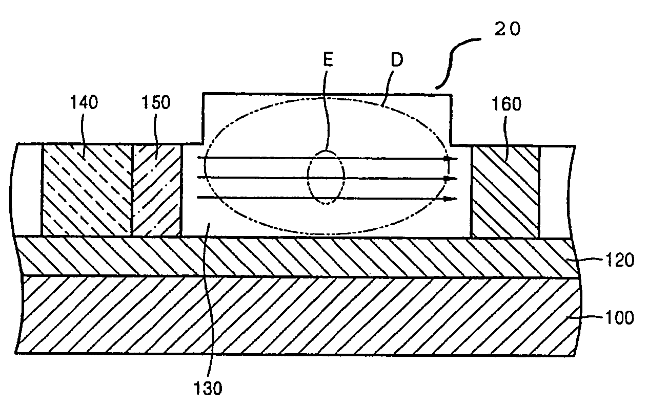
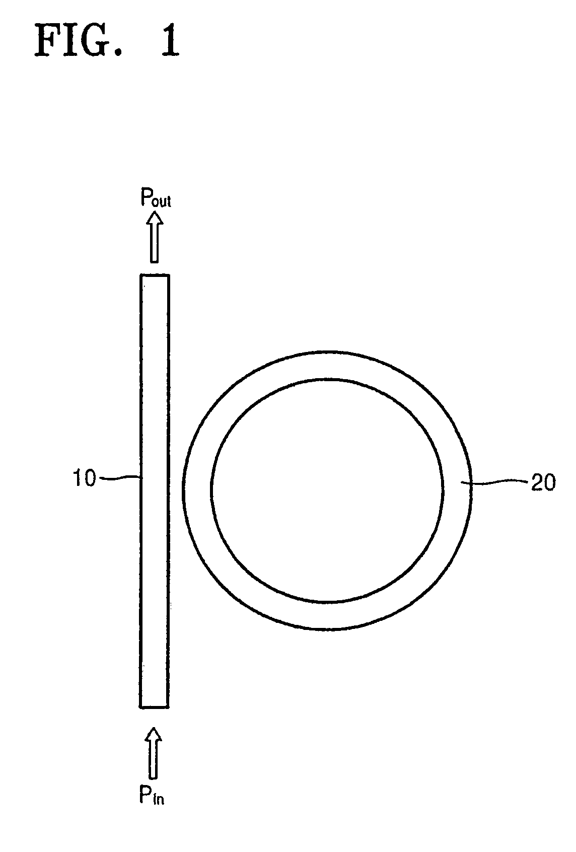
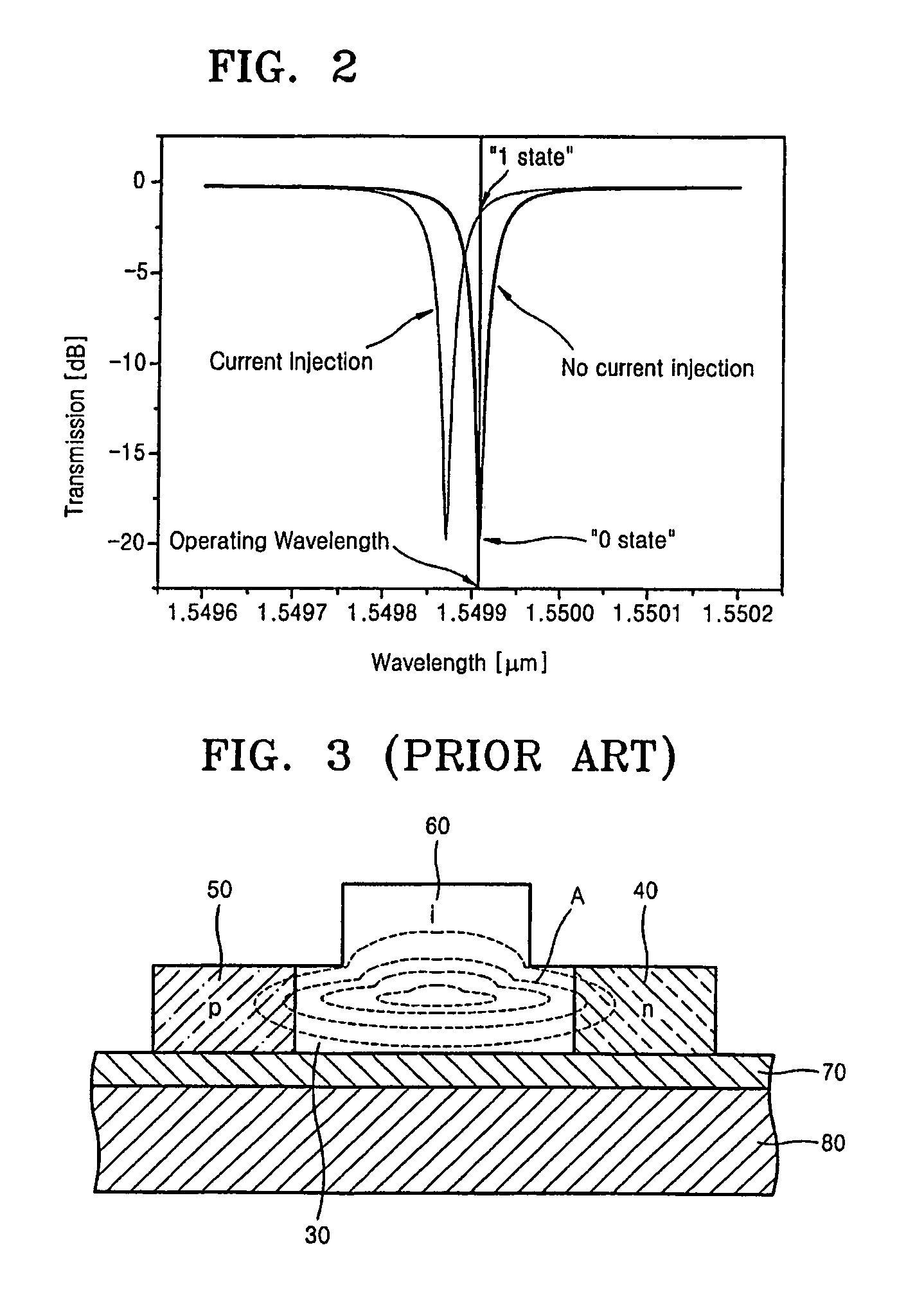
[0037]The present invention will now be described more fully with reference to the accompanying drawings, in which exemplary embodiments of the invention are shown. The invention may, however, be embodied in many different forms and should not be construed as being limited to the embodiments set forth herein; rather, these embodiments are provided so that this disclosure will be thorough and complete, and will fully convey the concept of the invention to those skilled in the art. In the drawings, the thicknesses of layers and regions are exaggerated for clarity. It will also be understood that when a layer is referred to as being “on” another layer or substrate, it can be directly on the other layer or substrate, or intervening layers may also be present. Like reference numerals in the drawings denote like elements. The terms used herein are for illustrative purpose of the present invention only and should not be construed to limit the meaning or the scope of the present invention a...


PUM

PropertyMeasurementUnit
refractive indexaaaaaaaaaa

Abstract

Provided is a high-speed ring optical modulator based on a silicon semiconductor, having increased optical modulation speed. The high-speed ring optical modulator includes a ring optical waveguide including a portion in which the refractive index varies, that is, a refractive index variation portion, and an optical waveguide having a constant refractive index. The refractive index variation portion comprises a bipolar transistor. Thus carriers can be supplied to and discharged from the refractive index variation portion, through which light is transmitted, at high speed, and thus the optical modulation speed can be increased.

Description

CROSS-REFERENCE TO RELATED PATENT APPLICATION[0001]This application claims the benefit of Korean Patent Application No. 10-2006-0096455, filed on Sep. 29, 2006 in the Korean Intellectual Property Office, the disclosure of which is incorporated herein in its entirety by reference.BACKGROUND OF THE INVENTION[0002]1. Field of the Invention[0003]The present invention relates to a silicon semiconductor-based optical device, and more particularly, to a silicon semiconductor-based optical device including an optical waveguide having refractive index variation.[0004]2. Description of the Related Art[0005]Due to the rapid development in silicon semiconductor technology, the speed of semiconductor chips such as computer CPUs, DRAMs, and SRAMs is increasing. However, despite this, the signal communication speed between semiconductor chips has not increased accordingly. In order to address this problem, semiconductor chip communication using light has been suggested.[0006]First, connecting semi...

Claims


Application Information

Patent Timeline
Patent Type & Authority Patents(United States)
IPC IPC(8): G02F1/035G02B6/26
CPCG02F1/015G02F2001/0152G02F2203/15G02F1/025G02F1/3133G02F1/0152G02B6/10G02F1/00
Inventor PARK, JEONG WOOKIM, GYUNGOCKKIM, HYUN SOOMHEEN, BONGKI
Owner ELECTRONICS & TELECOMM RES INST
Why Eureka
Try Eureka