High resolution delay line architecture

a delay line and high resolution technology, applied in the field of high resolution delay line architecture, can solve the problems of reducing the resolution of delay lines, increasing duty cycle distortion, and multiplication/buffer design, and achieve the effect of minimal duty cycle distortion and higher resolution

Inactive Publication Date: 2007-02-01
BROADCOM INT PTE LTD
View PDF9 Cites 1 Cited by
  • Summary
  • Abstract
  • Description
  • Claims
  • Application Information

AI Technical Summary

Benefits of technology

[0004] In accordance with the teachings of the present invention, a delay line architecture is presented. The delay l

Problems solved by technology

There are several disadvantages to the multiplexer/buffer design.
For example, a multiplexer/buffer design architecture reduces delay line resolution (i.e., ability to individually control each delay line) and increases duty cycle distortion.
This is a substantial problem when clock signals are propagated through the multiplexer/buffer design and the rise time of the clock signal is different from the fall time of the clock signal.
In addition, to the du

Method used


Image

  • High resolution delay line architecture
  • High resolution delay line architecture

Examples


Embodiment Construction

[0010] While the present invention is described herein with reference to illustrative embodiments for particular applications, it should be understood that the invention is not limited thereto. Those having ordinary skill in the art and access to the teachings provided herein will recognize additional modifications, applications, and embodiments within the scope thereof and additional fields in which the present invention would be of significant utility.

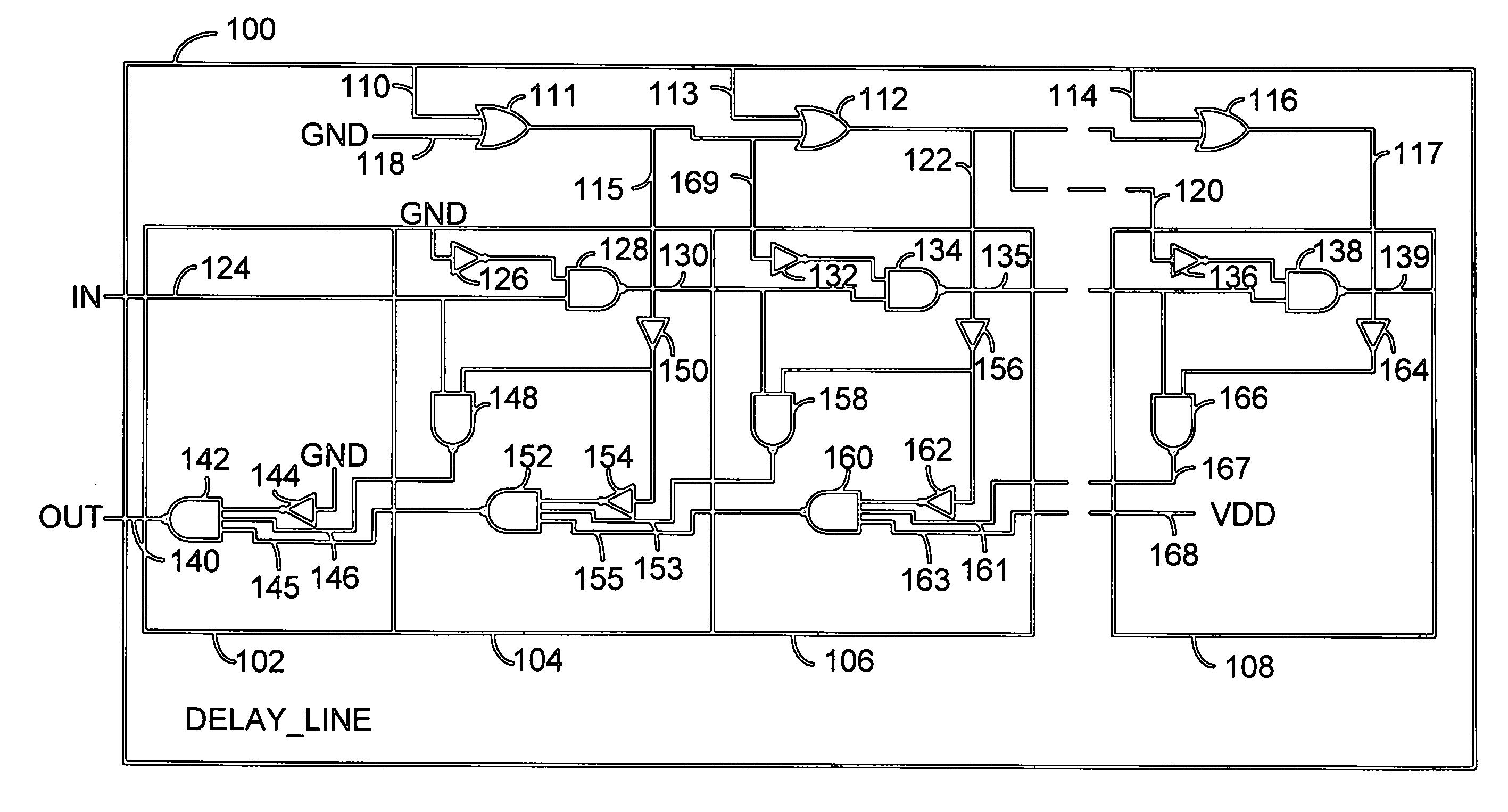
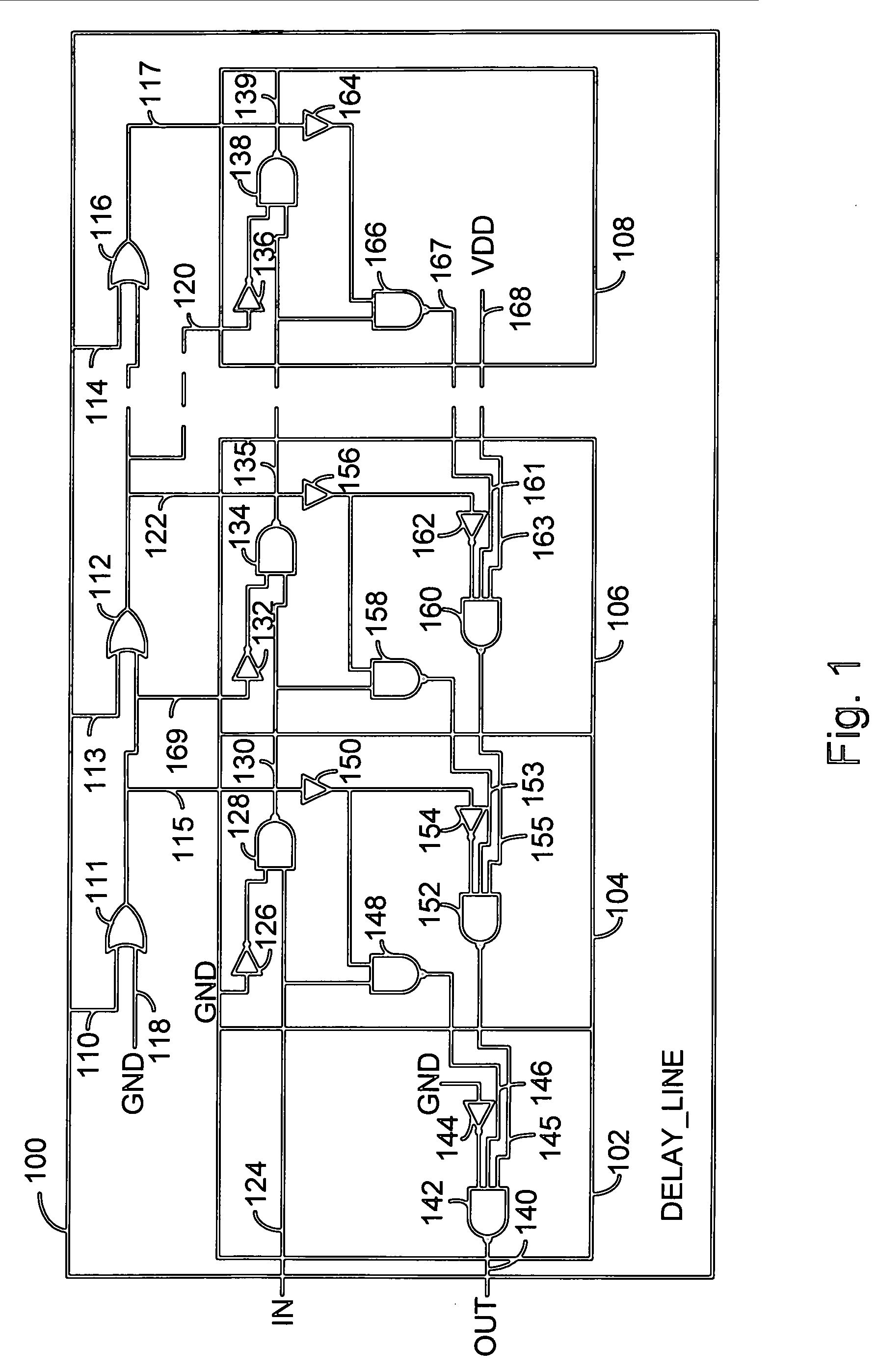
[0011] The building block of a delay line is the delay element. In accordance with the teachings of the present invention a delay element is implemented with three NAND gates. The NAND gates are configured to balance any differences between rise and fall times. This is accomplished by implementing an equal amount of rise and fall transitions through each delay element gate, balancing out any differences between rise and fall times. As a result, the three NAND gate design for the delay element greatly reduces duty cycle distortion. I...


PUM


Abstract

A delay line architecture is presented. In one embodiment, the delay line is used to introduce delay compensation into a circuit design at the top level of the circuit design.

Description

BACKGROUND OF THE INVENTION Description of the Related Art [0001] In conventional memory controllers, memory processors are built into an integrated circuit design and used to control data rate transfers to and from an external random access memory (RAM). Delay lines are used to delay the chip and RAM clocks by a certain amount to guarantee reliable transfer of data to and from the RAM. Many conventional delay line architectures include a multiplexer / buffer design. [0002] There are several disadvantages to the multiplexer / buffer design. For example, a multiplexer / buffer design architecture reduces delay line resolution (i.e., ability to individually control each delay line) and increases duty cycle distortion. Duty cycle distortion occurs when the rise time of the leading edge of a signal propagated through the multiplexer / buffer design is different from a fall time of the falling edge of a signal propagated through the multiplexer / buffer design. This is a substantial problem when c...

Claims


Application Information

Patent Timeline
IPC IPC(8): H03H11/26
CPCH03K2005/00234H03K5/131
Inventor HAUGESTUEN, BENJAMIN
Owner BROADCOM INT PTE LTD
Why Eureka
Try Eureka