Infrared imager

a technology of infrared imager and imager body, which is applied in the field of infrared imager, can solve the problems of increased and the inability to widely use imagers, and achieves the effects of increasing the size, weight and power consumption of the imager, and increasing the cost of additional electronics and display apparatuses

Inactive Publication Date: 2007-02-08
HER MAJESTY THE QUEEN AS REPRESENTED BY THE MINIST OF NAT DEFENCE OF HER MAJESTYS CANADIAN GOVERNMENT
View PDF4 Cites 20 Cited by
  • Summary
  • Abstract
  • Description
  • Claims
  • Application Information

AI Technical Summary

Benefits of technology

[0008] It is a further object of the invention to provide an infrared imager that is compact, reliable, and converts infrared radiation directly to a visible image.

Problems solved by technology

However, the imagers are still not widely used due to cost, size, weight and power consumption.
These additional electronics and display apparatuses incur additional cost, along with increased size, weight and power consumption.
This turn-on voltage is not standard to CMOS technology.
This electrostatic force may pull or collapse the cantilever if the turn-on voltage cannot be kept low.
This requirement creats extra difficulties for the electronics.
Third, moving parts always add uncertain reliability to the system, especially in a harsh environment.
Fourth, the radiation has to pass through the substrate in order to reach the cantilever structure and, as a result, at least 50% of the radiation is lost.
First, the operation of QWIPs requires cryocoolers, which are sizable and power hungry.
Second, the LED of this proposal is buried under the surface.
Emitted light from the LED is severely diverged when it reaches the top layer.
This makes the coupling between the QWIP-LED to the CCD camera difficult.
Third, at least 50% of the incident radiation is lost in the substrate before reaching the QWIP.
However, similar to the previous approaches, this method carries the shortcomings of power loss in the substrate and unreliability of moving parts.

Method used


Image

  • Infrared imager
  • Infrared imager
  • Infrared imager

Examples


Embodiment Construction

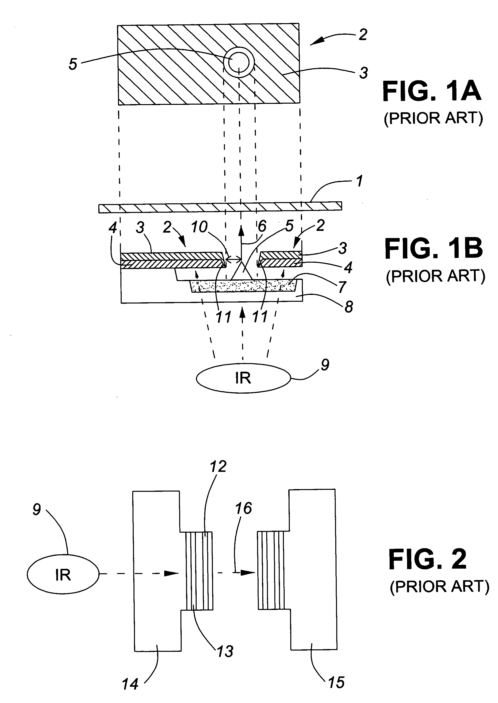
[0022] There are a few proposed solutions to minimize the electronics and visually display an image for infrared imagers. For example, a direct view infrared structure was disclosed in U.S. Pat. No. 6,140,646, by Heinz Busta et al wherein an electrode 11 on a cantilever 2, which is made of two layers 3 and 4 of material or bi-material, with different thermal expansion coefficients, is used to modulate electron emissions from an array of field emitters 5 as illustrated in FIG. 1b. The emitted electrons (arrow 6) then bombard a phosphor plate 1, giving a visible image. FIG. 1b shows a cross sectional view of that configuration whereas FIG. 1a is a top view. When IR radiation is incident on the bi-material cantilever 2, which usually consists of a layer of conductive film 3 and a layer of insulator 4 having different thermal expansion coefficients, the cantilever 2 bends as its temperature rises in response to absorbed infrared radiation. This bending changes the distance 10 between th...


PUM


Abstract

An infrared imager for detecting infrared (IR) radiation of a scene in a field of view (FOV) of an optical system and converting the IR into a visible image wherein the imager consists of an array of uncooled microbolometers in a focal plane of the optical system and a array of light emitting diode (LED) or liquid crystal display (LCD) elements. The IR radiation collected by the microbolometer produces a change in an electrical output applied to electronic circuitry connected to the array of LED s or LCDs. The electronic circuitry controls the intensity of a LED element or the reflectance of an LCD element. As a result, the imager converts the infrared radiation from the scene into visible light. The light reflected from the LCD or produced by LEDs in an array constitutes the scene image

Description

FIELD OF THE INVENTION [0001] The present invention relates generally to an infrared imager having an array of uncooled microbolometers containing a layer of infrared (IR) sensitive material which upon absorption of infrared (IR) radiation modulates a visual display to provide a visible image, according to the amount of IR radiation absorbed by each microbolometer and, in particular, to an imager that provides a direct conversion of infrared radiation of a scene into a visible one for observation. BACKGROUND OF THE INVENTION [0002] Infrared imagers are becoming increasingly important for commercial and non-commercial applications such as night vision imaging. However, the imagers are still not widely used due to cost, size, weight and power consumption. For example, traditional night vision imagers, such as cryogenically cooled HgCdTe or InSb focal plane array imagers, uncooled bolometer or pyroelectric thermal imagers, require intervening electronics to convert the absorbed infrare...

Claims


Application Information

Patent Timeline
Patent Type & Authority Applications(United States)
IPC IPC(8): H01L25/00
CPCH01L27/14632H04N5/33H01L27/14669
Inventor LAOU, PHILIPSNGO PHONG, LINH
Owner HER MAJESTY THE QUEEN AS REPRESENTED BY THE MINIST OF NAT DEFENCE OF HER MAJESTYS CANADIAN GOVERNMENT
Why Eureka
Try Eureka