LED package and method for fabricating the same

a technology of led packages and led components, applied in the direction of basic electric elements, electrical equipment, semiconductor devices, etc., can solve the problems of exponential reduction of the performance of such led packages, poor heat dissipation properties of above-described conventional led packages, and poor heat dissipation performance of led packages, etc., to achieve superior heat dissipation performance, simple construction, and high power

Inactive Publication Date: 2007-02-08
SAMSUNG DISPLAY CO LTD
View PDF3 Cites 31 Cited by
  • Summary
  • Abstract
  • Description
  • Claims
  • Application Information

AI Technical Summary

Benefits of technology

[0015] Accordingly, the present invention has been made to solve the above and other problems occurring in the prior art, and an exemplary object of the present invention is to provide an LED package having superior in heat dissipation performance, which is suitable for packaging a high power LED package, and which is simple in construction, whereby the LED package can be applied to an LED with a complicated electrode structure.

Problems solved by technology

However, because the performance of such an LED is exponentially reduced as temperature increases, heat dissipation is also important.
The above-described conventional LED package has poor heat dissipation properties because it has a relatively long heat transfer path formed by contact between different materials (LED→insulation layer→heat spreading member→substrate), whereby thermal resistance increases.
Therefore, it is not suitable for packaging a high power LED.
However, the thermal resistance of the above-mentioned conventional LED package is naturally high because it has contact parts formed from different materials and because the heat transfer path of the LED package is long due to the thicknesses of the package and the substrate.
If the heat dissipation performance of an LED package is poor, the life of the LED will be shortened.
Furthermore, it may cause fatal damage to a system because parts around the LED package may deteriorate and become thermally deformed due to the high temperature of the LED package.
Accordingly, there is a problem in that the number of assembling steps is increased and thus the manufacturing costs are also increased.
Moreover, the step of interconnecting the electrodes and leads with conducting wires becomes more difficult as electrode patterns on LEDs become more complicated in order to improve the optical efficiency and performance of the LED.

Method used


Image

  • LED package and method for fabricating the same
  • LED package and method for fabricating the same
  • LED package and method for fabricating the same

Examples


Embodiment Construction

[0054] Hereinbelow, exemplary embodiments of the present invention are described in detail with reference to accompanying drawings. In the following description, detailed descriptions of known functions and configurations will be omitted when it may make the subject matter of the present invention rather unclear.

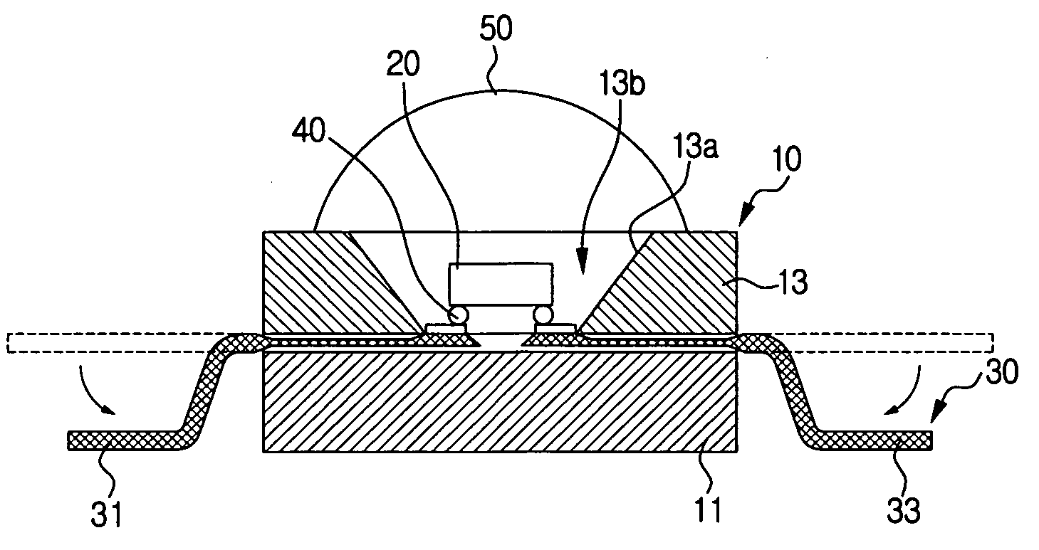
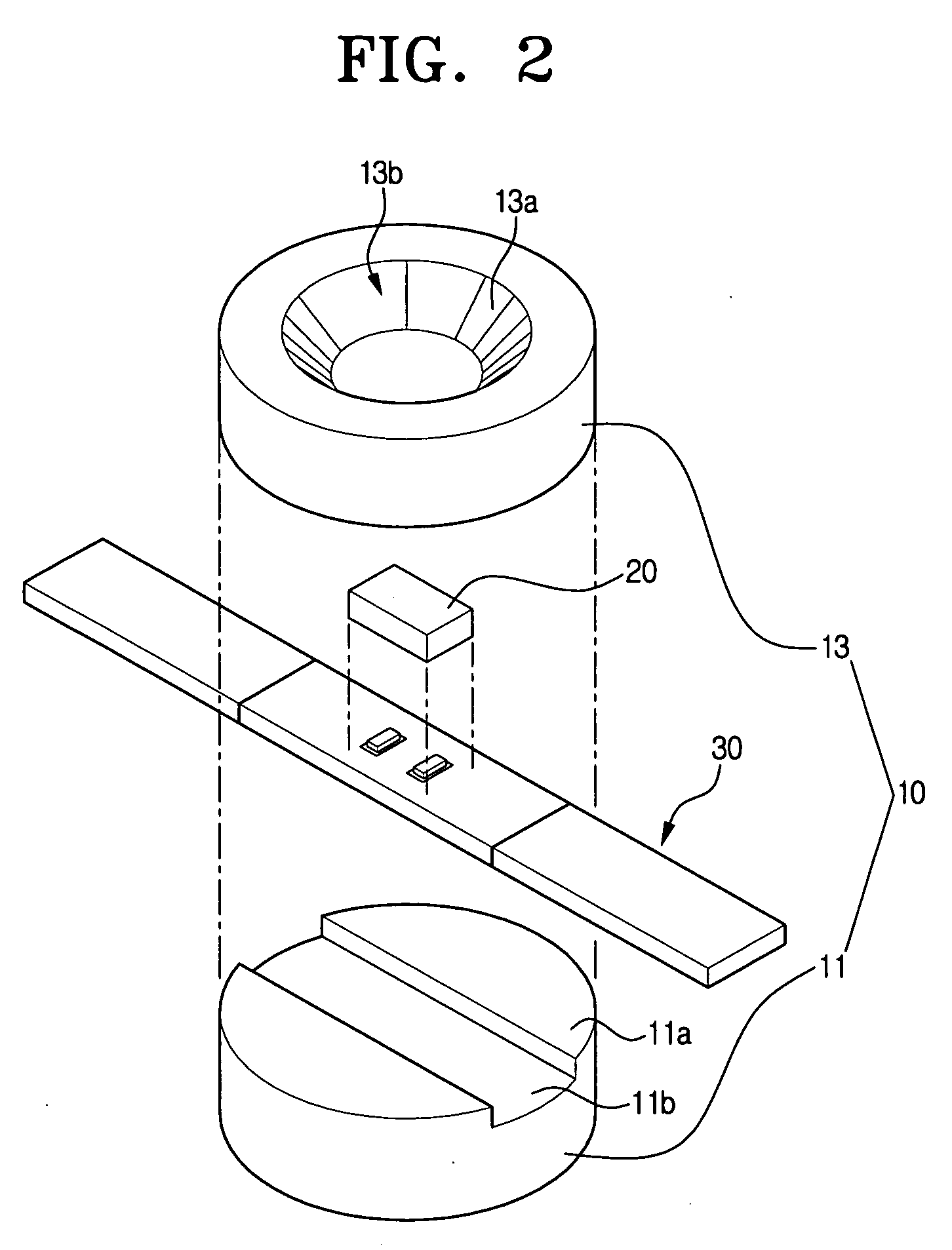
[0055] Referring to FIG. 2, an LED package according to a first exemplary embodiment of the present invention comprises a package body 10, an LED 20, and a lead 30, on which the LED is mounted and which is bonded to the package body 10.

[0056] The package body 10 comprises a base member 11 and a reflecting member 13 mounted on the base member 11. The base member 11 has a substantially circular cross-section and is formed from a metallic material having superior heat conductivity. A surface 11a of the base member 11, facing the reflecting member 13, includes a lead mounting part 11a. The lead mounting part 11b is formed by etching a portion of the surface 11a of the base mem...


PUM


Abstract

An LED package comprises: a package body having therein a LED receiving part including a reflecting surface; an LED mounted within the LED receiving part; a lead mounted within the package body such that first and second ends of the lead are exposed to the outside of the package body. The lead includes first and second conductive parts which are electrically connected to the LED and a non-conductive part which insulates the first and second conductive parts from each other.

Description

CROSS-REFERENCE TO RELATED APPLICATIONS [0001] This application claims the benefit of Korean Patent Application No. 2005-71366 filed Aug. 4, 2005 in the Korean Intellectual Property Office, the disclosure of which is incorporated herein by reference. BACKGROUND OF THE INVENTION [0002] 1. Field of the Invention [0003] Apparatuses and methods consistent with present invention relate to a light emitting diode (LED) package and a manufacturing method thereof, which can be used for illumination or as a back light unit of a liquid crystal display (LCD) or the like. [0004] 2. Description of the Related Art [0005] LEDs are widely employed not only in the electric and electronic fields but also in the advertisement field due to their advantages in terms of long life and low power consumption. Attempts to employ LEDs, for example, as backlight units of LCDs, have been made recently, and the LEDs may be widely employed in indoor and outdoor illumination systems in the future. Therefore, an int...

Claims


Application Information

Patent Timeline
Patent Type & Authority Applications(United States)
IPC IPC(8): H01L33/00H01L33/58H01L33/60H01L33/62H01L33/64
CPCH01L25/0753H01L33/486H01L33/62H01L33/64H01L2224/73265H01L2224/48247H01L2224/48091H01L2224/16245H01L2924/00014H01L2924/00
Inventor SHIN, SU-HOSHIN, KYU-HOKWEON, SOON-CHEOLMOON, CHANG-YOULCHOI, JIN-SEUNG
Owner SAMSUNG DISPLAY CO LTD
Why Eureka
Try Eureka