Memory module and method thereof

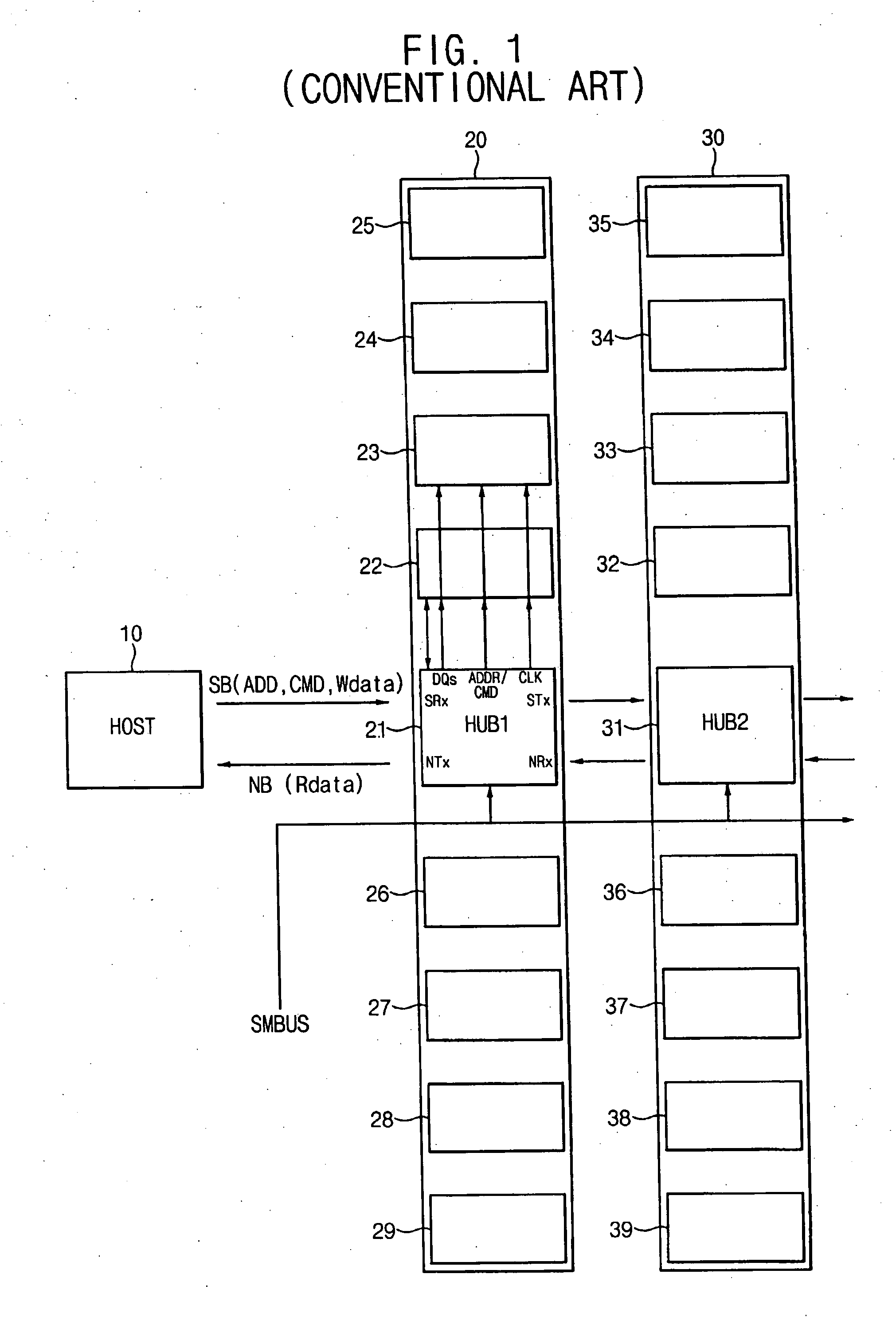
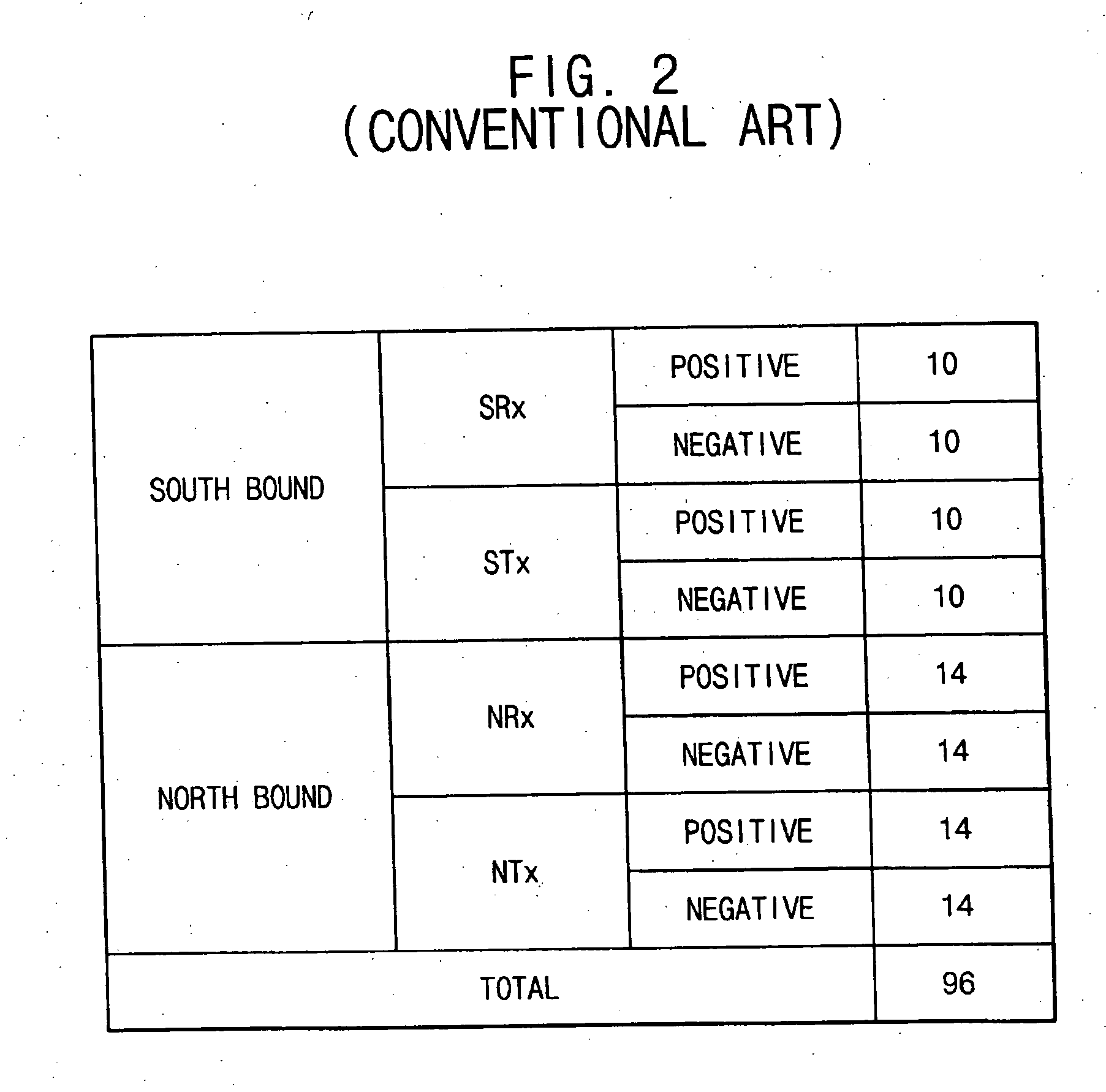
a memory module and memory module technology, applied in the field of memory module and method of testing the memory module, can solve the problems of reducing the efficiency of conventional transparent mode memory test, unable to test the 72 dq pins and 18 dqs pins through 24 channels, and difficulty in determining whether the defect has occurred in one of the hubs.

Inactive Publication Date: 2007-02-08
SAMSUNG ELECTRONICS CO LTD
View PDF8 Cites 12 Cited by
  • Summary
  • Abstract
  • Description
  • Claims
  • Application Information

AI Technical Summary

Benefits of technology

[0039] In addition, example embodiments of the present invention provide a method for t...

Problems solved by technology

However, if the higher-speed test equipment detects a defect in a tested memory module, it may be difficult to determine whether the defect has occurred in one of the hubs 21/31 or within the memory chips 22 through 29 and/or 32 through 39.
However, because an input/output (IO) of the FBDIMM may include 72 DQ pins (e.g., 8 DQ pins per memory chip×9 memory...

Method used


Image

  • Memory module and method thereof
  • Memory module and method thereof
  • Memory module and method thereof

Examples


Embodiment Construction

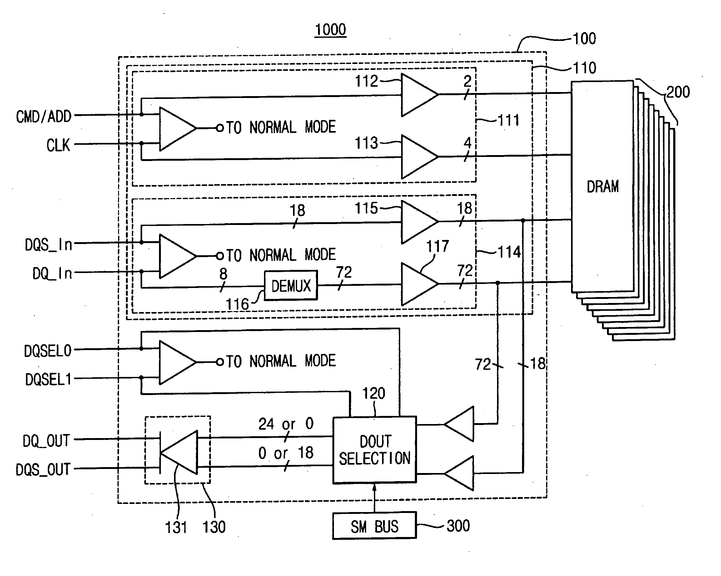
[0051] Hereinafter, example embodiments of the present invention will be explained in detail with reference to the accompanying drawings.

[0052] It will be understood that, although the terms first, second, etc., may be used herein to describe various elements, these elements should not be limited by these terms. These terms are used to distinguish one element from another. For example, a first element could be termed a second element, and, similarly, a second element could be termed a first element, without departing from the scope of example embodiments of the present invention. As used herein, the term “and / or” includes any and all combinations of one or more of the associated listed items.

[0053] It will be understood that when an element is referred to as being “connected” or “coupled” to another element, it can be directly connected or coupled to the other element or intervening elements may be present. In contrast, when an element is referred to as being “directly connected” ...


PUM


Abstract

A memory module and method thereof are provided. In the example method, a test signal may be applied to a plurality of memory chips included in the memory module. Output data from the plurality of memory chips may be received in response to the applied test signal. The received, output data may be divided into a plurality of groups. At least one of the plurality of groups may be selected in response to an output group selection signal. The at least one selected group may be output (e.g., to an external device). The example memory module may include a plurality of chips and a hub. The example memory module may be configured to perform the above-described example method.

Description

PRIORITY STATEMENT [0001] This application claims priority under 35 U.S.C. § 119 to Korean Patent Application No. 2005-71198 filed on Aug. 4, 2005, the contents of which are herein incorporated by reference in its entirety. BACKGROUND OF THE INVENTION [0002] 1. Field of the Invention [0003] Example embodiments of the present invention relate generally to a memory module and method thereof, and more particularly to a memory module and method of testing the memory module. [0004] 2. Description of the Related Art [0005] Memory chips, such as dynamic random-access memory (DRAM) chips, may be installed in a computer system in the form of memory modules. Each memory module may include a plurality of the memory chips mounted on a printed circuit board (PCB). [0006] Memory modules may typically be as one of a classified single inline memory module (SIMM) or a dual inline memory module (DIMM). Memory chips may be mounted on one side of a PCB in the SIMM and memory chips may be mounted on bot...

Claims


Application Information

Patent Timeline
IPC IPC(8): H04L12/26
CPCG11C5/04G11C2029/2602G11C29/08G11C29/00
Inventor SHIN, SEUNG-MANSHIN, HUI-CHONGLEE, JONG-GEONHAN, KYUNG-HEE
Owner SAMSUNG ELECTRONICS CO LTD
Why Eureka
Try Eureka