Planarization method for manufacturing semiconductor device

a semiconductor and planarization technology, applied in semiconductor/solid-state device manufacturing, basic electric elements, electric devices, etc., can solve problems such as undesired attacks on semiconductor substrates, damage to sog ild b>120/b>, and complicating a process

Inactive Publication Date: 2007-02-08
SK HYNIX INC
View PDF3 Cites 14 Cited by
  • Summary
  • Abstract
  • Description
  • Claims
  • Application Information

AI Technical Summary

Benefits of technology

[0047] The present invention provides a planarization method for manufacturing a semiconductor device, which prevents stepped portions of a target layer, to be planarized, due to the topology of a layer under the target layer, and defects in planarizing the target layer caused thereby.

Problems solved by technology

Further, the SOG ILD 120 is damaged by chemicals during a subsequent cleaning process.
Thereby, it is possible to cause undesired attacks against the semiconductor substrate 160 made of silicon.
However, the above method requires additional steps, thus complicating a process for forming the isolation layer and increasing costs to perform the process.
However, the above method requires expensive ceria based slurry and a new supply device for the ceria based slurry.

Method used


Image

  • Planarization method for manufacturing semiconductor device
  • Planarization method for manufacturing semiconductor device
  • Planarization method for manufacturing semiconductor device

Examples


Embodiment Construction

[0059] Now, preferred embodiments of the present invention will be described in detail with reference to the annexed drawings.

[0060] FIGS. 4 to 7 are sectional views illustrating a planarization method for fabricating a semiconductor device in accordance with one embodiment of the present invention.

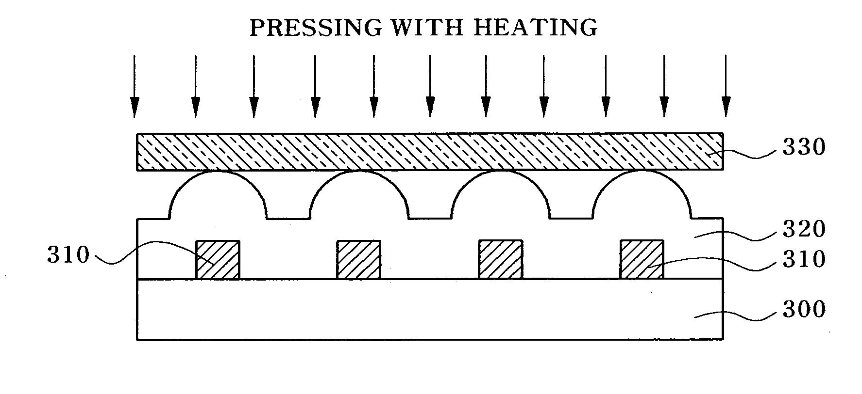
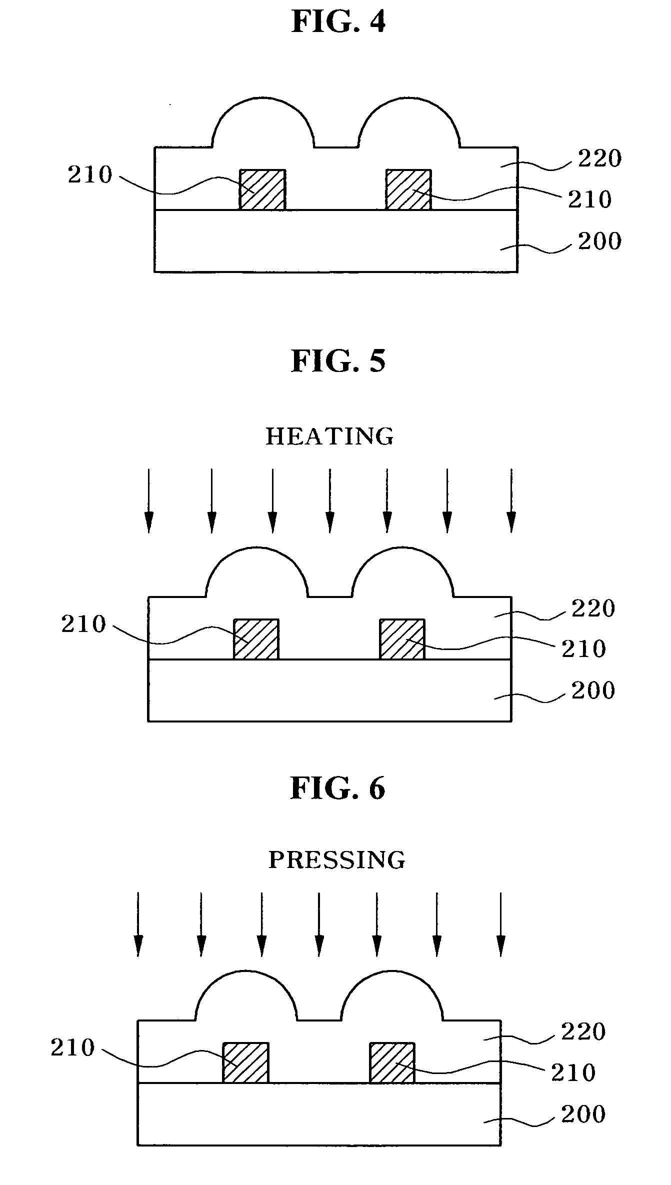
[0061] With reference to FIG. 4, patterns 210 are disposed on a lower layer 200, and a target layer 220 is disposed on the lower layer including the patterns 210. Here, the lower layer 200 may be an ILD or a semiconductor substrate. The target layer 220 is a layer to be planarized, and preferably an ILD layer.

[0062] The target layer 220 to be planarized is made of a material having flowability at more than a designated temperature, which does not exceed 300° C. For example, the target layer 220 is made of a photo-cured material, a thermosetting material, or thermoplastic material. That is, the target layer 220 is made of a material, which exhibits flowability by applying heat or light ...


PUM


Abstract

A method for planarizing a layer of a semiconductor device includes heating the layer to exhibit flowability, and applying pressure through an optically flat surface layer onto the layer to planarize the layer. And the planarizing method further comprises etch-back or chemical-mechanical polishing on the planarized layer.

Description

BACKGROUND [0001] The present invention relates to semiconductor devices, and more particularly to a planarization method and methods for forming an interlayer dielectric layer (ILD), an isolation layer, and contact plugs using the planarization method. [0002] In fabrication of a semiconductor device, a planarization method using chemical mechanical polishing (CMP) is mainly used. In the above planarization method using CMP, a mechanical action and a chemical action are simultaneously carried out, so they interact with each other. [0003] More specifically, a wafer is polished using a pad and slurry. A table provided with the pad is simply rotated. A head is simultaneously rotated and vibrated while pressure of a designated intensity is applied to the head. The wafer is mounted on the head via surface tension or vacuum. The surface of the wafer contacts the pad by the load of the head and the pressure applied to the head, while slurry flows into a fine gap between the contact surface...

Claims


Application Information

Patent Timeline
Patent Type & Authority Applications(United States)
IPC IPC(8): H01L21/461H01L21/311H01L21/302
CPCH01L21/31051H01L21/3212H01L21/31058H01L21/31053
Inventor CHOI, YONG SOO
Owner SK HYNIX INC
Why Eureka
Try Eureka