Fabrication method of substrate with charge trap and insulating buried layer

A charge trap and insulating buried layer technology, which is applied in the manufacture of circuits, electrical components, semiconductors/solid-state devices, etc., can solve the problems of device circuit signal loss, weaken the high-resistance characteristics of the support layer, etc., and achieve the effect of reducing difficulty

Active Publication Date: 2019-03-29
SHANGHAI SIMGUI TECH
View PDF11 Cites 0 Cited by
  • Summary
  • Abstract
  • Description
  • Claims
  • Application Information

AI Technical Summary

Problems solved by technology

Parasitic capacitance can cause loss of device circuit signal
Moreover, the inversion layer on the surface area of ​​the support layer close to the insulating layer can still allow carriers to flow, thus weakening the high resistance characteristics of the support layer

Method used


Image

  • Fabrication method of substrate with charge trap and insulating buried layer
  • Fabrication method of substrate with charge trap and insulating buried layer
  • Fabrication method of substrate with charge trap and insulating buried layer

Examples


Embodiment Construction

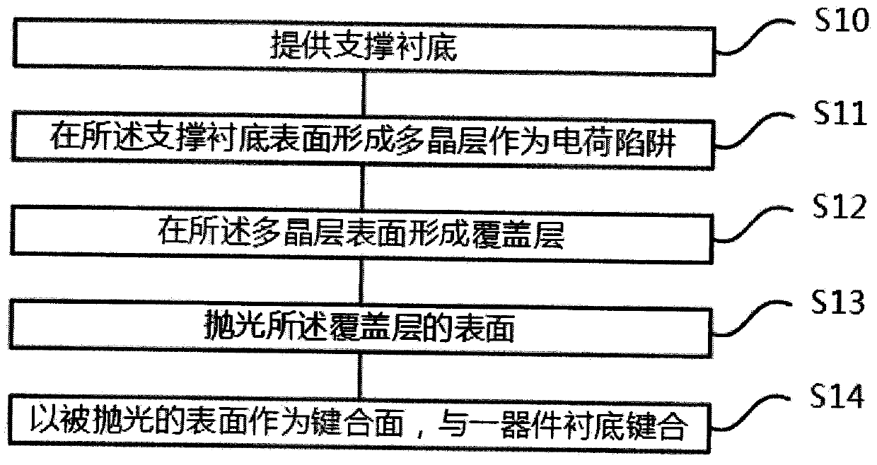
[0013] The specific implementation of the method for preparing a substrate with a charge trap and an insulating buried layer provided by the present invention will be described in detail below in conjunction with the accompanying drawings.

[0014] attached figure 1 Shown is a schematic diagram of the implementation steps of this specific embodiment, including: step S10, providing a support substrate; step S11, forming a polycrystalline layer on the surface of the support substrate as a charge trap; step S12, forming a charge trap on the surface of the polycrystalline layer Forming a cover layer; step S13, polishing the surface of the cover layer; step S14, using the polished surface as a bonding surface, and bonding with a device substrate.

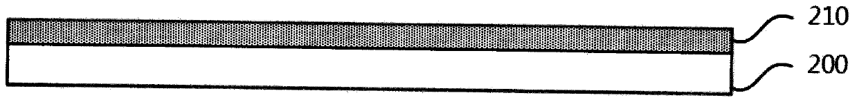
[0015] attached Figure 2A to attach Figure 2D Shown is the process schematic diagram of this specific embodiment.

[0016] attached Figure 2A As shown, and referring to step S10, a supporting substrate 200 is provided. The suppor...


PUM

PropertyMeasurementUnit
thicknessaaaaaaaaaa

Abstract

The invention provides a preparation method for a substrate with a charge trap and an insulation buried layer, comprising the following steps: providing a support substrate; forming a polycrystal layer on the surface of the support substrate to be used as the charge trap; forming a covering layer on the surface of the polycrystal layer, wherein the covering layer is non-crystal insulation material; polishing the surface of the covering layer; and taking the polished surface as a bonding surface, and bonding with a device substrate. The preparation method for the substrate has the advantages that: the non-crystal insulation covering layer is adopted as the bonding surface, so that direct polishing and bonding on the polycrystal layer are avoided, and the difficulty in polishing and bonding is lowered.

Description

technical field [0001] The invention relates to the field of semiconductor materials, in particular to a method for preparing a substrate with a charge trap and an insulating buried layer. Background technique [0002] A typical substrate structure with an insulating buried layer in the prior art includes three layers, successively a support layer, an insulating layer on the surface of the support layer, and a device layer on the surface of the insulating layer. [0003] If the above substrate is used in the radio frequency field, more stringent requirements are imposed on the electrical properties of the substrate. The transmission of the radio frequency signal in the device layer will form a parasitic circuit in the support layer, thus receiving crosstalk from the support layer. And as the frequency increases, the effect of crosstalk becomes more and more obvious. The current way to solve this problem is to use a high-resistance substrate as a support layer. The high-res...

Claims


Application Information

Patent Timeline
Patent Type & Authority Patents(China)
IPC IPC(8): H01L21/02
CPCH01L21/02123H01L21/02592H01L21/02595
Inventor 叶斐陈猛陈国兴张峰
Owner SHANGHAI SIMGUI TECH
Why Eureka
Try Eureka