Apparatus for manufacturing chip-type ceramic electronic component and method for manufacturing chip-type ceramic electronic component

A technology for electronic components and manufacturing devices, which is applied to the manufacturing device of chip-type ceramic electronic components and the manufacturing field of chip-type ceramic electronic components, can solve the problems of easy generation of chips, cracks, etc., and achieves prevention of adhesion, improved productivity, The effect of high connection reliability

Active Publication Date: 2011-03-23
MURATA MFG CO LTD
View PDF2 Cites 0 Cited by
  • Summary
  • Abstract
  • Description
  • Claims
  • Application Information

AI Technical Summary

Problems solved by technology

[0010] First of all, there is a problem that in the case of using the operation method of spraying polishing particles such as sandblasting used in the above-mentioned Patent Documents 1 and 2, since the polishing particles suddenly collide with the end faces of the chip-type components, there are cases where fine cracks are caused. , and, since it needs to be carried out in a closed device in such a way that the polishing particles do not scatter, the device is enlarged.
[0011] Also, as disclosed in the above-mentioned Patent Document 2, in the state where a plurality of chip-type components are collectively held in the following form, when polishing is performed using a polishing member having a polishing agent such as a polishing cloth, a polishing wheel, or a wire brush, although The end face of the chip-type component can be polished, but there is a problem that the polishing member cannot be wound around the side surface of the chip-type component at the same time to perform chamfering of the ridge line, and this form is to align the end faces and the side surfaces of each chip-type component without gaps join
In addition, since the ridges of the chip-type components are polished with the edges protruding, there is a problem that chips are likely to be generated on the ridges.

Method used


Image

  • Apparatus for manufacturing chip-type ceramic electronic component and method for manufacturing chip-type ceramic electronic component
  • Apparatus for manufacturing chip-type ceramic electronic component and method for manufacturing chip-type ceramic electronic component
  • Apparatus for manufacturing chip-type ceramic electronic component and method for manufacturing chip-type ceramic electronic component

Examples


Embodiment Construction

[0091] Embodiments of the present invention are shown below, and their characteristic features will be described in more detail.

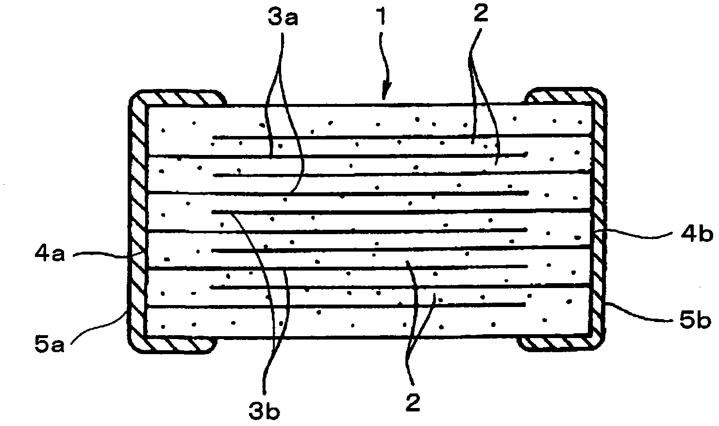
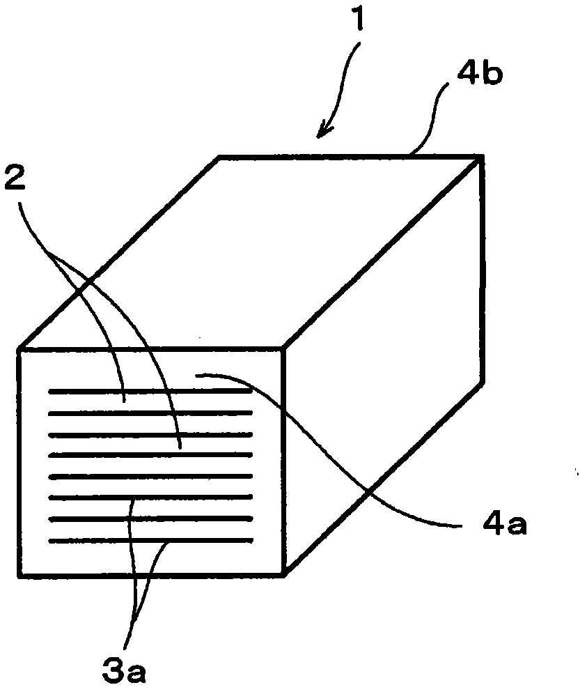
[0092] In this embodiment, description will be made taking as an example the case of manufacturing a laminated ceramic capacitor having the following configuration, for example, as figure 1 As shown, a pair of external electrodes 5a, 5b are arranged on the facing end surfaces 4a, 4b of the ceramic element (chip type element) 1 in a manner to conduct with the internal electrode layers 3a, 3b, wherein the ceramic element (chip type element) A plurality of internal electrode layers 3 a , 3 b are disposed so as to face each other across a ceramic layer (dielectric layer) 2 .

[0093] Furthermore, in this embodiment, when manufacturing the above-mentioned multilayer ceramic capacitor, as figure 1 , figure 2As shown, the following chip-type element (ceramic element) 1 is prepared: the internal electrode layers 3a, 3b and the ceramic layer 2 are alte...


PUM


Abstract

A chip-type ceramic electronic component, which is to be manufactured through a step of polishing an end surface, can be efficiently manufactured by efficiently polishing an end surface of a chip-type element, while eliminating generation of cracks and chipping by relatively simple configuration. Provided is an apparatus for manufacturing a chip-type ceramic electronic component, which is to be manufactured through a step of polishing a pair of facing end surfaces (4a, 4b) of a chip-type element (1) having ceramic as a material. The apparatus is provided with a holding member (10), which arranges and holds the chip-type elements (1) such that the chip-type elements are spaced apart from each other with one of the pair of end surfaces (4a, 4b) of each chip-type element on the same flat surface; a polishing brush (20) wherein a brush holder (24) holds a brush main body (23), which has a polishing material embedded in a flexible resin; and a driving mechanism (30) which drives the polishing brush (20) so that the brush main body slides on the one end surface in a state where the brush main body is brought into contact with the one end surface of the chip-type element.

Description

technical field [0001] The present invention relates to a manufacturing device of a chip-type ceramic electronic component and a manufacturing method of a chip-type ceramic electronic component. A method of manufacturing a chip-type ceramic electronic component manufactured by the processing step, and a manufacturing apparatus of a chip-type ceramic electronic component used in the manufacturing method. Background technique [0002] A multilayer ceramic electronic component represented by a multilayer ceramic capacitor has a structure in which a plurality of ceramic layers and internal electrode layers are stacked, and the internal electrode layers are alternately led out on both ends of the element body (chip type element) facing each other. External electrodes are arranged on the end faces so as to be electrically connected to the internal electrode layers. [0003] However, chip-type devices are generally formed by firing an unfired laminate in which ceramic layers and i...

Claims


Application Information

Patent Timeline
Patent Type & Authority Applications(China)
IPC IPC(8): H01G4/30H01G4/12H01G4/252H01G13/00
CPCH01G4/30H01G4/12H01G13/00
Inventor 佐藤浩司肴仓俊树真田幸雄青木健一
Owner MURATA MFG CO LTD
Why Eureka
Try Eureka