Circuit board and method for manufacturing the same

Inactive Publication Date: 2007-02-08
SAMSUNG ELECTRONICS CO LTD
View PDF16 Cites 26 Cited by
  • Summary
  • Abstract
  • Description
  • Claims
  • Application Information

AI Technical Summary

Benefits of technology

[0010] Accordingly, embodiments of the present invention provide a circuit board which has improved operational characteristics, and a method for manufacturing a circuit board having the improved operational characteristics.

Problems solved by technology

However, because it is difficult to control the characteristic impedance of the via, signal distortion may occur.
If the distance between the pair of signal patterns varies, an impedance mismatch may occur and, as a result, the signal may be reflected causing signal distortion.

Method used


Image

  • Circuit board and method for manufacturing the same
  • Circuit board and method for manufacturing the same
  • Circuit board and method for manufacturing the same

Examples


Embodiment Construction

[0024] Reference will now be made in greater detail to exemplary embodiments of the invention, which are illustrated in the accompanying drawings. Wherever possible, the same reference numerals will be used throughout the drawings and the description to refer to the same or like parts.

[0025] A circuit board according to the present invention may include a PCB (printed circuit board), an FPCB (flexible PCB), an FRPCB (flexible rigid PCB), or a ceramic substrate, but is not limited to such examples. For the sake of explanatory convenience, a PCB will be exemplified in the following detailed description.

[0026] The circuit board of the present invention may be adapted to a package board, a multi-chip module board, or a general-type motherboard, but again is not limited to such examples.

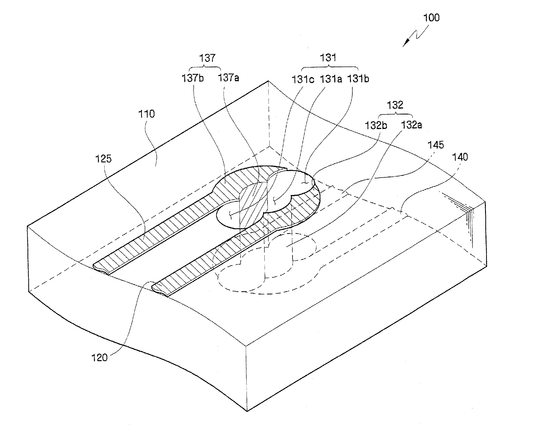
[0027]FIGS. 3 and 4 are respectively a perspective view and a plan view illustrating a via structure adopted in a circuit board in accordance with an embodiment of the present invention, and FIG. 5 is ...


PUM


Abstract

A circuit board and a method of manufacturing the same are disclosed. Embodiments of the circuit board may include a dielectric substrate, a first via structure comprising a first via-hole, which is defined through the dielectric substrate, and a plurality of first vias that are formed on an inner wall of the first via-hole and to connect a plurality of signal patterns positioned on the upper and lower surfaces of the dielectric substrate.

Description

[0001] This application claims priority from Korean Patent Application No. 10-2005-0067448 filed on Jul. 25, 2005, in the Korean Intellectual Property Office, the disclosure of which is incorporated by reference. BACKGROUND [0002] 1. Field of the Invention [0003] The present invention relates, in general, to a circuit board and a method for manufacturing the same, and more particularly to a circuit board which has improved operational characteristics, and a method for manufacturing the same. [0004] 2. Description of the Prior Art [0005] As semiconductor devices become highly integrated, miniaturized, and high-speed, the functionality of the circuit boards used in these devices becomes more important. Specifically, it is important to design a circuit board capable of preventing signal distortion. In a circuit board, complicated signal patterns can be stably formed in a multi-layered structure in such a way as to be stacked over one another, and signal patterns formed in different lay...

Claims


Application Information

Patent Timeline
IPC IPC(8): G01R31/28
CPCH05K1/0237H05K1/115H05K3/0047H05K3/403H05K2203/1476H05K2201/09236H05K2201/09536H05K2201/09645H05K3/429H05K1/11
Inventor PARK, SUNG-JOOLEE, JAE-JUNSO, BYUNG-SELEE, JUNG-JOON
Owner SAMSUNG ELECTRONICS CO LTD
Why Eureka
Try Eureka