

Nano tube cell, and semiconductor device having nano tube cell and double bit line sensing structure
- Summary
- Abstract
- Description
- Claims
- Application Information
AI Technical Summary
Benefits of technology
Problems solved by technology
Method used
Image

Examples
Embodiment Construction
[0021] A nano tube cell, and a cell array circuit having the nano tube cell and a double bit line sensing structure in accordance with a preferred embodiment of the present invention will now be described in detail with reference to the accompanying drawings.
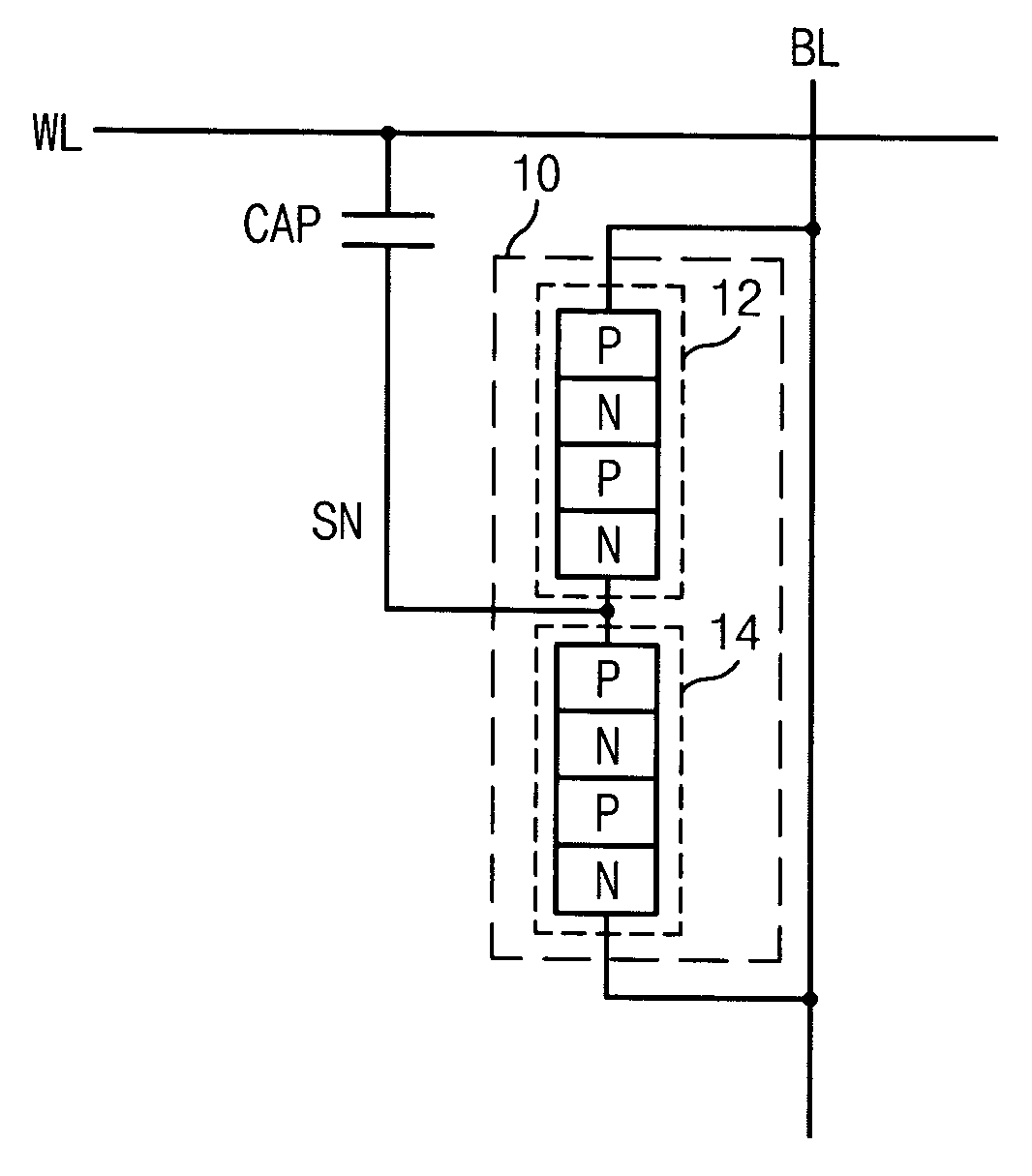
[0022]FIG. 1 is a circuit diagram illustrating a unit nano tube cell in accordance with the preferred embodiment of the present invention.
[0023] The nano tube cell includes one capacitor CAP and one PNPN diode switch 10.
[0024] The capacitor CAP stores cell charges corresponding to a cell data. One side electrode of the capacitor CAP is coupled to a word line WL, and the other side electrode thereof is coupled to a node SN. In the PNPN diode switch 10, a pair of serial PNPN tubes 12 and 14 are connected in parallel to a bit line BL, and the node SN is formed between the serial PNPN tubes 12 and 14. That is, an N terminal of the PNPN tube 12 and a P terminal of the PNPN tube 14 are commonly connected to the node SN, and a P ter...
PUM
 Abstract
Description
Claims
Application Information