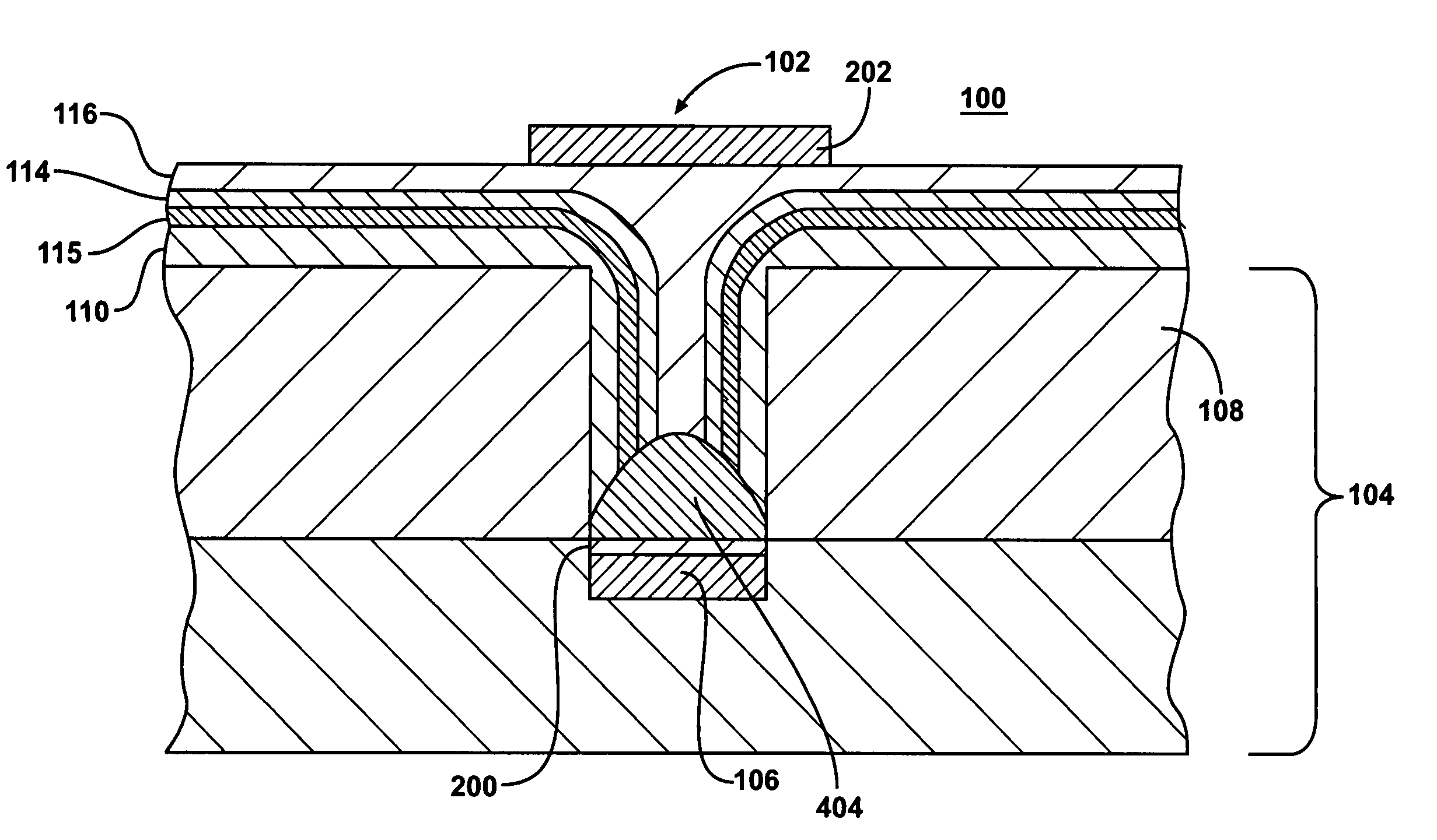
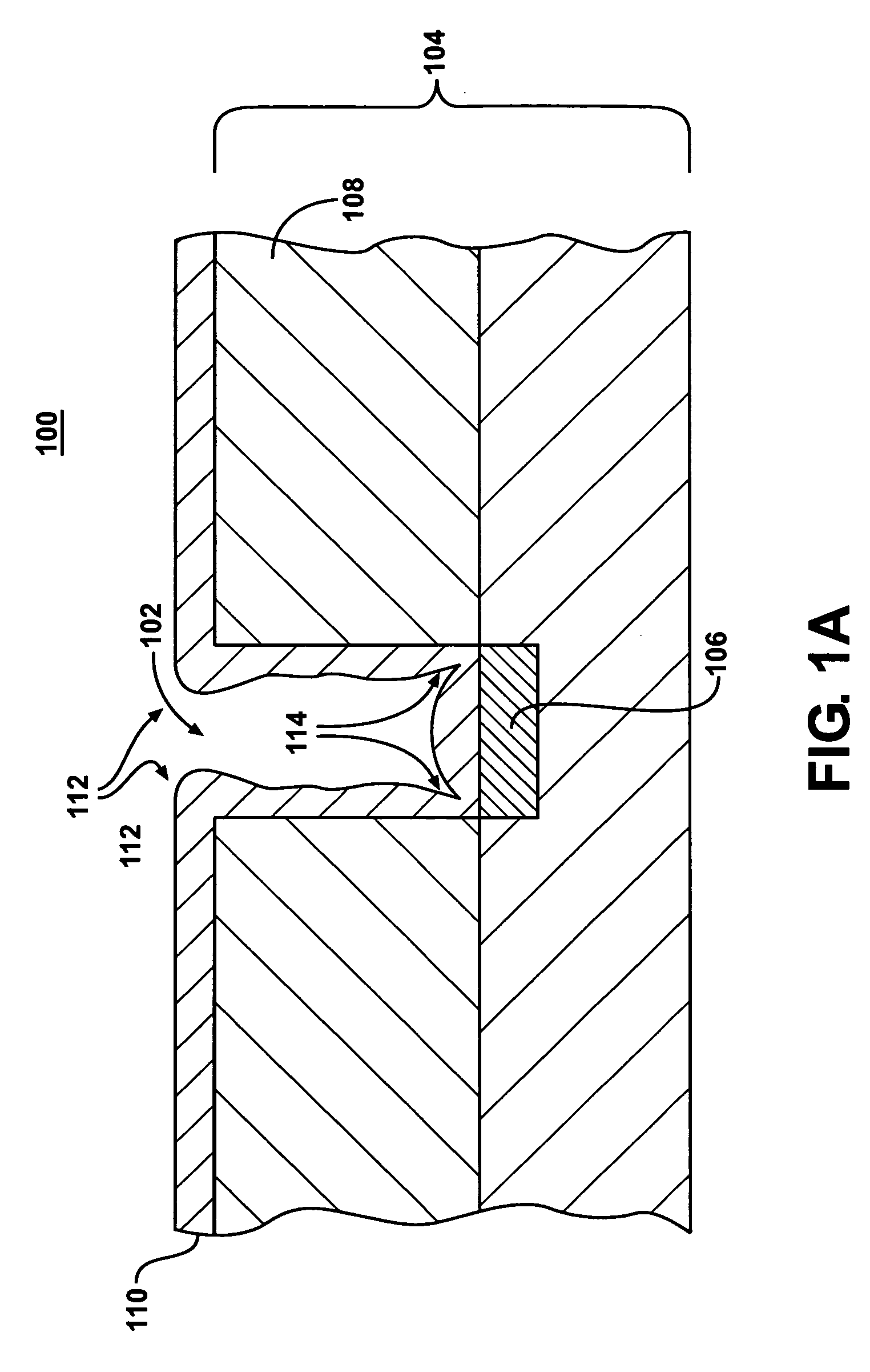
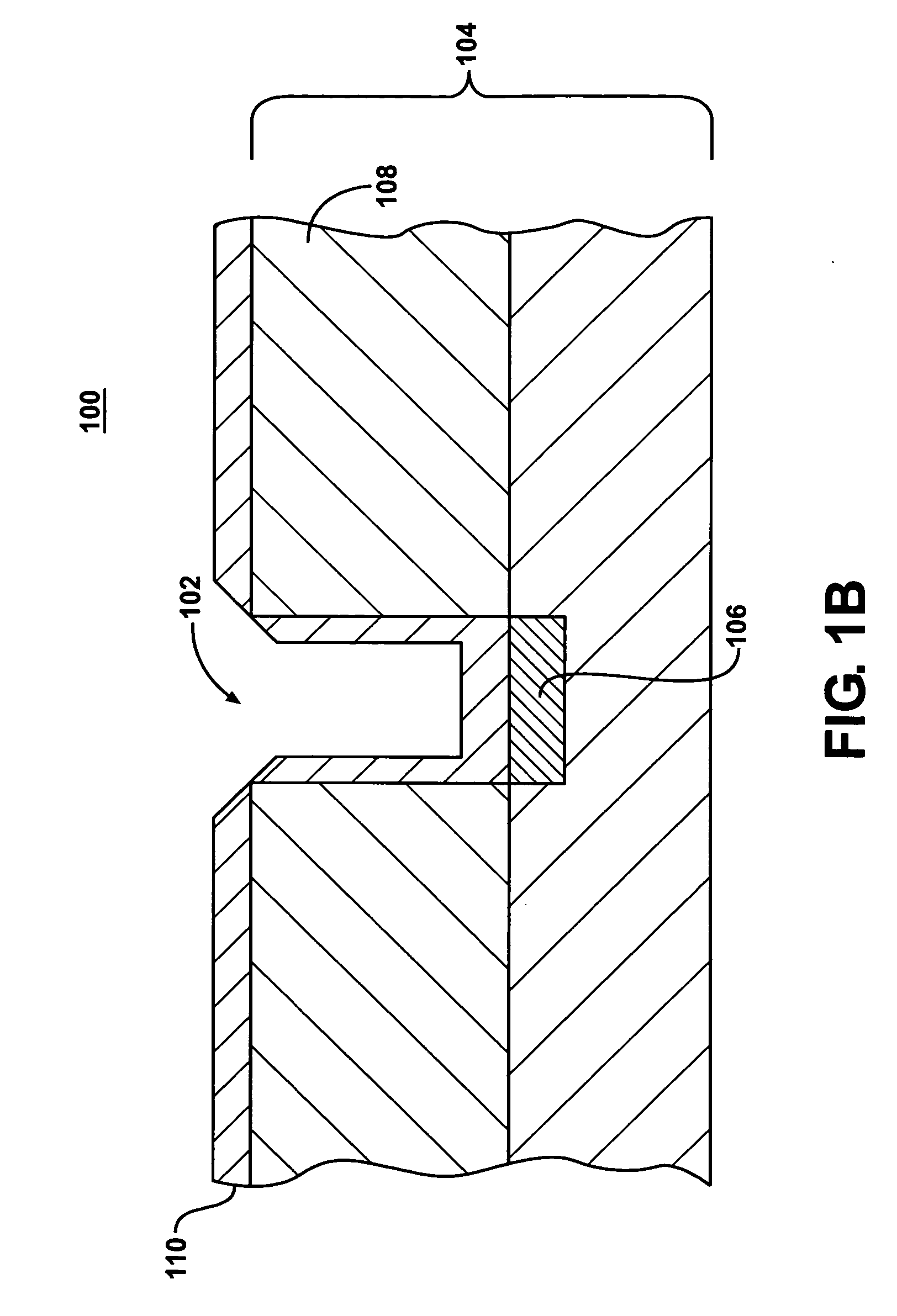
[0008]The non-
planar substrate may, for example, be substantially planar, with openings formed to accept the deposited
phase change material. Such openings in the substrate may take the form of pores, vias, micro-trenches or dashes formed within the substrate, for example.
Phase change materials may be combined to improve operational characteristics such as cycle life,
data retention, RESET current, SET speed, multi-level operation, or
resistance drift, for example. Materials having different characteristics may be combined in a manner that emphasizes the performance of one type of
phase change material within a region of the memory element within which
programming takes place, and emphasizes the characteristics of another type of
phase change material outside that “
active volume.” For example, a
phase change material associated with the
active volume may be selected for its fast SET speed, whereas phase change material that is to lie outside the
active volume may be selected for its high
thermal resistance. Alternatively, materials having different characteristics may be included within the active volume to, for example, improve the multi-level characteristics of a memory.
[0010]In an illustrative embodiment, high-resistance phase change material, material which may include
Nitrogen or SiO2, for example, is deposited into an opening in a substrate then etched back to produce a desired profile. A different phase change material, having a lower resistance, is then deposited on the etched first layer of phase change material. The higher resistance of the lower layer encourages formation of the active volume within the lower layer. The lower resistance of the upper layer reduces the overall SET resistance of the
resultant memory cell. At the same time, the upper layer of phase change material is a better thermal insulator than a top
electrode and, as a result, the upper layer of phase change material operates to confine heat to an active volume in the bottom layer and thereby reduce operating current requirements.
[0012]The structural, chemical, and electrical characteristics of a multi-layer
phase change memory may be optimized, employing at least one etch step, to enhance multi-level
memory operation by, for example, producing a structure that diminishes the
cell's overall sensitivity to
programming current in the transition region between the SET and RESET states. Typically, the transition from the SET to RESET is accomplished by applying a
current pulse of only slightly higher magnitude than a pulse that would not affect the state of the device; there is an abrupt change between SET and RESET.
Programming the
cell to states that are intermediate to the SET and RESET states requires precise control of
programming currents. By diminishing the
cell's sensitivity to programming current in the transition region, each state between the SET and RESET states may programmed with greater margin. In a multi-layer embodiment, materials featuring varying properties may be deposited in sequence to produce a cell within which the active volume encompasses at least a segment of each of the material
layers. A cell that is composed of multiple
layers may have a more
gradual transition from set to reset resistance as the differing segments of phase change materials become involved in the cell programming thereby providing greater margin for each programmed state.

