Light emitting display device

a display device and light-emitting technology, applied in the direction of discharge tube luminescnet screens, discharge tube/lamp details, cathode ray tubes/electron beam tubes, etc., can solve the problems of low efficiency of electron beam use, low reliability, low luminance and efficiency, etc., to reduce the excitation loss of electron beam, reduce image quality, and increase luminance and efficiency

Inactive Publication Date: 2007-02-15
HITACHI DISPLAYS
View PDF2 Cites 6 Cited by
  • Summary
  • Abstract
  • Description
  • Claims
  • Application Information

AI Technical Summary

Benefits of technology

[0006] It is therefore an object of the present invention to provide a light emitting display device employing the electron beam convergence method having not lowering of image quality by color mixing, reducing the excitation loss of the electron beam, increasing the luminance and efficiency, and reducing the cost.
[0009] According to the present invention, it is possible to obtain a preferable display quality having no color mixing. Since no electron beam spread exists, a highly accurate panel can be configured. Moreover, all the electron beam emitted hit the phosphor. That is, there is no electron beam excitation loss and it is possible to improve the efficiency and luminance.

Problems solved by technology

However, the use efficiency of the electron beam is low, which in turn lowers the luminance and efficiency.
Moreover, insulative (ceramic) barrier is charged by the irradiation of the electron beam, which causes discharge and lowers reliability.
Moreover, in the cold cathode field electron emission display device disclosed in JP-A-2003-197132, the method for providing a protrusion on the gate electrode has a high electron beam convergence effect and less lowering of the use efficiency of the electron beam.
However, it is necessary to form / treat the gate electrode, which complicates a process, increases the cost, and lowers the throughput and yield.

Method used


Image

  • Light emitting display device
  • Light emitting display device
  • Light emitting display device

Examples


embodiment 1

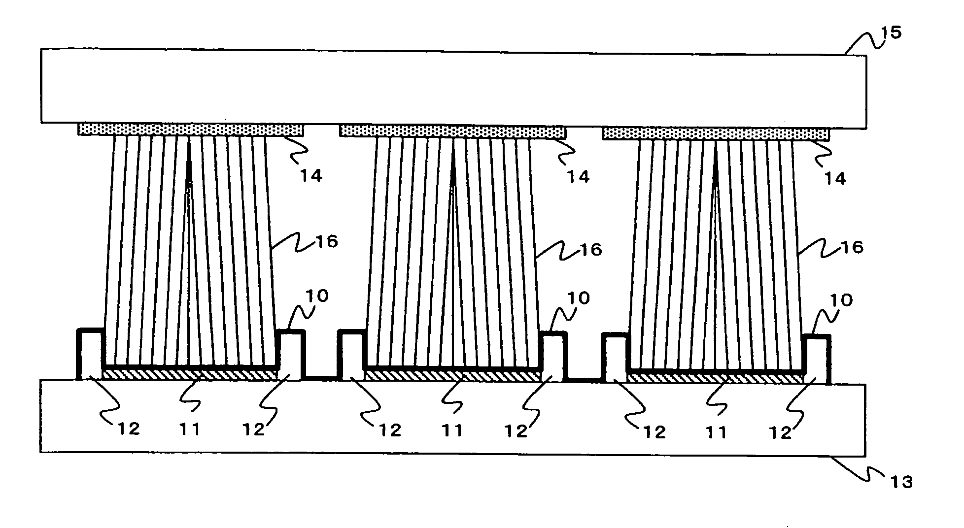
[0027]FIG. 1 is a partial cross sectional view of pixels in a light emitting display device according to an embodiment of the present invention. MIM is used as an electron emitter element 11 which is surrounded by a conductive barrier 12 (scanning wire).

[0028] The electron emitter element 11 is surrounded by a barrier 12 of the same potential as the cathode potential. At least a surface of the barrier 12 is formed by a conductive layer so that the surface potential of the barrier 12 and the electron emitter element 11 are identical. That is, the electron emitter element 11 and the barrier 12 are covered by an upper electrode 10.

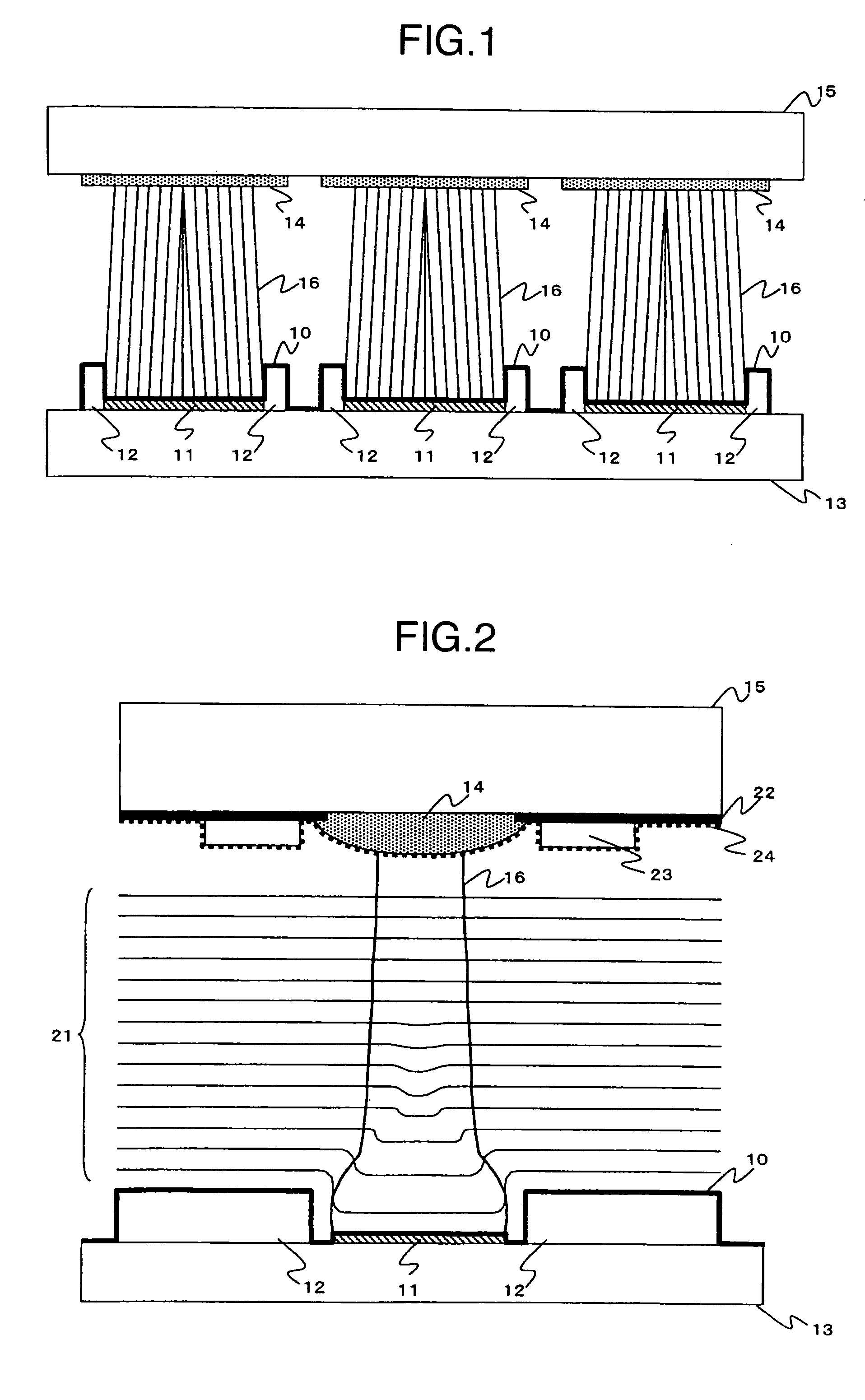
[0029] The electron emitter element 11 and the barrier 12 are formed on a cathode substrate 13. An anode substrate 15 having R (red), G (green), and B (blue) color phosphor 14 opposes to the cathode substrate 13. The color phosphors 14 are excited to emit colors by the electron beam 16 emitted from the electron emitter element 11.

[0030]FIG. 2 is a conceptu...

embodiment 2

[0039] This embodiment shows a specific pixel structure for easily realizing the Embodiment 1. In addition to this, this embodiment has a structure for increasing the electron beam displacement and reducing the affect of spacer bonding member required for the display panel structure to the electron beam displacement. Moreover, this embodiment does not irradiate a phosphor of an adjacent pixel even there is a minute amount of electron beam which has not been converged.

[0040]FIG. 4 shows a planar structure of a pixel. FIG. 5 shows a cross sectional view of a pixel in which the positions shown by arrows A, B, C, D correspond to the positions A, B, C, D in FIG. 4. The electron emitter element 11 is provided in the groove 42 of the scanning wire 41, i.e., the groove 42 of the upper electrode 10 of the scanning wire 41. The electron emitter element 11 is selected by the scanning wire 41 and the signal wire 49 and emits an electron beam 16.

[0041] In FIG. 4, the distance from the peripher...

embodiment 3

[0049]FIG. 7A shows a pixel configuration employing the SED (surface-conduction electron-emitting display) and FIG. 7B is a conceptual diagram of the pixel circuit. As shown in FIG. 7A, two platinum display electrodes 72, 73 connected to the scanning wire 41 and the signal line 49 are exposed to an opening 71 of the inter-layer insulation film 53 and a PbO pattern is formed between the display electrodes.

[0050] The SED element 74 is surrounded by the opening 75 of the scanning wire 41. As shown in FIG. 7B, the SED element 74 is surrounded by the barrier 12 connected to the scanning wire 41, thereby forming an electron lens using the scanning wire 41 as the barrier 12. It should be noted that the opening 75 may be arranged at the signal wire. In this case, the barrier 12 has a potential different from that of the scanning wire 41. Accordingly, it is possible to obtain a greater electron beam convergence effect.


PUM


Abstract

In a light emitting display device using electron emitter elements, it is possible to prevent lowering of image quality caused by spread of electron beams. MIM (Metal Insulator Metal) is used as the electron emitter elements and each of the electron emitter elements is surrounded by a conductive barrier (scanning wire). The electron emitter elements and the barriers are covered by upper electrodes so that the barriers and the surfaces of the electron emitter elements have the same electrical potential. The electron emitter elements and the barriers are formed on a cathode substrate. Color phosphors of R (red), G (green), and B (blue) are formed on an anode substrate at the side opposing to the cathode substrate. The color phosphors are excited by electron beams emitted from the electron emitter elements.

Description

INCORPORATION BY REFERENCE [0001] The present application claims priority from Japanese application JP2005-230504 filed on Aug. 9, 2005, the content of which is hereby incorporated by reference into this application. BACKGROUND OF THE INVENTION [0002] The present invention relates to a light emitting display device for converging electron beams emitted from a plurality of cold cathodes arranged in a matrix shape, causing the fluorescent surface to emit light, and displaying an image. [0003] Various structures have been suggested for suppressing spread of an electron beam in the light emitting display device using a cold cathode as a planar electron source. For example, JP-A-2003-16924 discloses a field emission type electron source including a pixel structure having an insulative barrier on an electron source substrate for limiting spread of the electron beam emitted. Moreover, JP-A-2003-197132 discloses a cold cathode field electron emission display device including a spindt type e...

Claims


Application Information

Patent Timeline
Patent Type & Authority Applications(United States)
IPC IPC(8): H01J63/04H01J1/62
CPCH01J29/04H01J31/127H01J29/481H01J29/467
Inventor MIKAMI, YOSHIROSAGAWA, MASAKAZUNAKAMURA, TOMOKISHIRAI, SHOJI
Owner HITACHI DISPLAYS
Why Eureka
Try Eureka