Vertical cavity surface emitting laser device

Inactive Publication Date: 2007-02-15
CANON KK
View PDF13 Cites 74 Cited by
  • Summary
  • Abstract
  • Description
  • Claims
  • Application Information

AI Technical Summary

Benefits of technology

[0011] By using a photonic crystal mirror as a reflective mirror of a VCSEL, a mirror composed of a multilayer film having a large thickness of about several micrometers can be replaced by a mirror composed

Problems solved by technology

This problem becomes critical when the VCSEL is applied to light condensing with a lens.
In addition, a defect level is present within a photonic bandga

Method used


Image

  • Vertical cavity surface emitting laser device
  • Vertical cavity surface emitting laser device
  • Vertical cavity surface emitting laser device

Examples


first embodiment

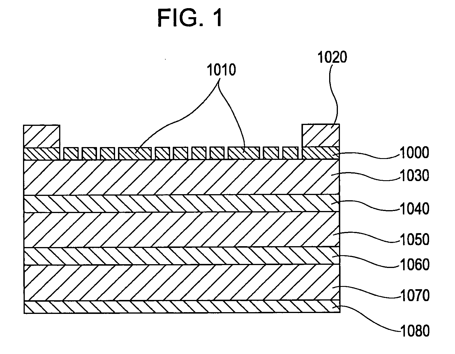
[0134] The structure of a laser device according to a first embodiment will now be described with reference to FIG. 6.

[0135] A lower cavity mirror light confinement layer 62, a lower cavity mirror layer 63, a lower cladding layer 64, an active layer 65, an upper cladding layer 66, and an upper cavity mirror layer 67 are sequentially laminated on a substrate 61. An n-electrode 68 and a p-electrode 69 are provided on the reverse face of the substrate 61 and on the top face of the upper cavity mirror layer 67, respectively.

[0136] The substrate 61 is an n-type GaAs substrate having a thickness of 565 μm. The lower cavity mirror light confinement layer 62 is composed of n-type Al0.7Ga0.4As and has a thickness of 1 μm. The lower cavity mirror layer 63 is composed of n-type Al0.4Ga0.6As and the lower cladding layer 64 is composed of n-type (Al0.5Ga0.5)0.5In0.5P. The upper cavity mirror layer 67 is composed of p-type Al0.4Ga0.6As and the upper cladding layer 66 is composed of p-type (Al0....

second embodiment

[0156] The structure of a laser device according to a second embodiment will now be described with reference to FIG. 9. A lower cavity mirror light confinement layer 92, a lower cavity mirror layer 93, a lower cladding layer 94, an active layer 95, and an upper cladding layer 96 are sequentially laminated on a substrate 91. A current narrowing layer 99 is provided so as to surround a part of the lower cladding layer 94, the active layer 95, and a part of the upper cladding layer 96. An upper cavity mirror layer 910 is further laminated on the upper cladding layer 96. An n-electrode 911 and a p-electrode 912 are provided on the reverse face of the substrate 91 and on the top face of the upper cavity mirror layer 910, respectively. The substrate 91 is an n-type GaAs substrate having a thickness of 565 μm. The lower cavity mirror layer and the lower cladding layer are composed of n-type Al0.4Ga0.6As and (Al0.5Ga0.5)0.5In0.5P, respectively. The upper cavity mirror and the upper cladding...

third embodiment

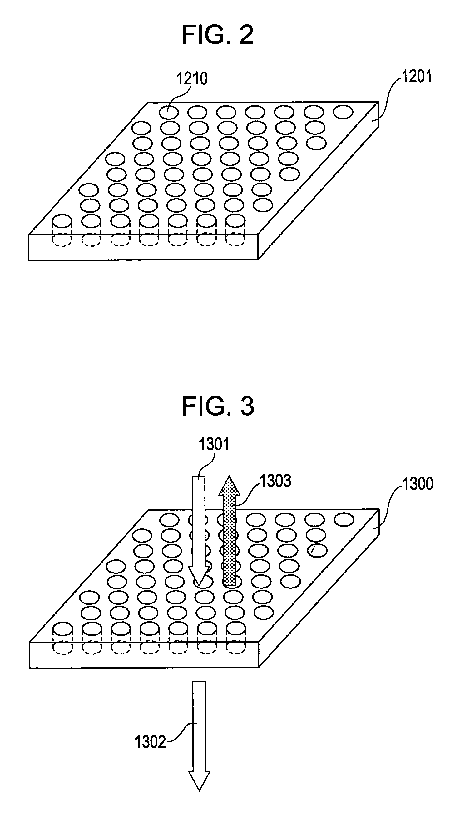
[0174] A third embodiment will now be described with reference to FIGS. 11A and 11B. Since the structure and the materials of the laser device itself are the same as those in the second embodiment, only the structure of the cavity mirrors will be described. The production process is also the same as that of the second embodiment.

[0175]FIGS. 11A and 11B are schematic views of lower and upper photonic crystal mirrors of the third embodiment, respectively, viewed from a direction perpendicular to a planer surface. As shown in FIG. 11A, in the lower cavity mirror, holes of a basic photonic crystal structure are provided in the entire surface, and defects formed by removing the holes are arrayed at the center. Parameters of the basic photonic crystal structure are the same as those of the lower cavity mirror of the second embodiment. This embodiment is characterized in the array of the defects. These defects are arrayed according to a specific regularity but arrayed aperiodically. Rough...


PUM


Abstract

A vertical cavity surface emitting laser device includes a first reflective mirror layer, a second reflective-mirror layer, and an active layer disposed therebetween, wherein at least one of the first reflective mirror layer and the second reflective mirror layer includes a periodic-refractive-index structure in which the refractive index periodically changes in the in-plane direction and a part of the periodic-refractive-index structure includes a plurality of parts that disorder the periodicity.

Description

BACKGROUND OF THE INVENTION [0001] 1. Field of the Invention [0002] The present invention relates to a vertical cavity surface emitting laser (VCSEL). [0003] 2. Description of the Related Art [0004] Vertical cavity surface emitting lasers are advantageous in terms of their low threshold value, ease of coupling with optical elements, possibility of formation of an array, and the like. Therefore, the VCSELs have been actively studied since the latter half of 1980's. [0005] However, the VCSELs are disadvantageous in that the spot size with which the VCSELs can oscillate in the single transverse mode is small, about 3 to 4 μm in diameter. The reason for this is as follows. When a VCSEL oscillates in the multimode, the responses for an optical element such as a lens are different from each other in each mode, and the emitted light does not behave in the same manner. [0006] Furthermore, since the gain region of the VCSEL is small, a pair of distributed Bragg reflector (DBR) mirrors consti...

Claims


Application Information

Patent Timeline
IPC IPC(8): H01S5/00
CPCH01S5/105H01S5/183H01S2301/166H01S5/18358H01S5/2063H01S5/18308H01S5/11
Inventor HORI, YUICHIROUCHIDA, MAMORUOKAMOTO, KOHEINAGATOMO, YASUHIROUCHIDA, TATSURO
Owner CANON KK
Why Eureka
Try Eureka