Efficient charge transferring in CMOS imagers

a technology of cmos imager and charge transfer efficiency, which is applied in the field of semiconductor devices, can solve the problems of poor charge transfer efficiency, fixed pattern noise and lag, and dark current, and achieve the effect of increasing the dynamic range of the pixel cell

Active Publication Date: 2007-03-01
APTINA IMAGING CORP
View PDF6 Cites 57 Cited by
  • Summary
  • Abstract
  • Description
  • Claims
  • Application Information

AI Technical Summary

Benefits of technology

[0014] In accordance with a second exemplary method of operating the pixel cell in accordance with the invention, a reset gate voltage fluctuates in a controlled manner, and the transfer gate signal is pulsed several times during the charge integration time. In one embodiment, a pulse is generated each time the reset gate voltage fluctuates. The method can also increase the dynamic range of the pixel cell.

Problems solved by technology

One common problem associated with conventional imager pixel cells, such as pixel cell 10, is dark current, that is, current generated due to electron generation / recombination collected in the photodiode 13 in the absence of light.
Dark current may be caused by many different factors, including: photodiode junction leakage, leakage along field isolation edges, transistor sub-threshold leakage, drain induced barrier lowering leakage, gate induced drain leakage, trap assisted tunneling, and pixel fabrication defects.
Another problem associated with conventional transfer gate technology involves fixed pattern noise and lag due to poor charge transfer efficiency.
Partially turning on the transfer gate 17 to minimize dark current, however, leads to fixed pattern noise and lag, as the potential barrier of the transfer gate may be too high to fully transfer all of the photo-generated charges.

Method used


Image

  • Efficient charge transferring in CMOS imagers
  • Efficient charge transferring in CMOS imagers
  • Efficient charge transferring in CMOS imagers

Examples


Embodiment Construction

[0026] In the following detailed description, reference is made to the accompanying drawings, which form a part hereof and illustrate specific embodiments in which the invention may be practiced. In the drawings, like reference numerals describe substantially similar components throughout the several views. These embodiments are described in sufficient detail to enable those skilled in the art to practice the invention, and it is to be understood that other embodiments may be utilized, and that structural, logical and electrical changes may be made without departing from the spirit and scope of the present invention.

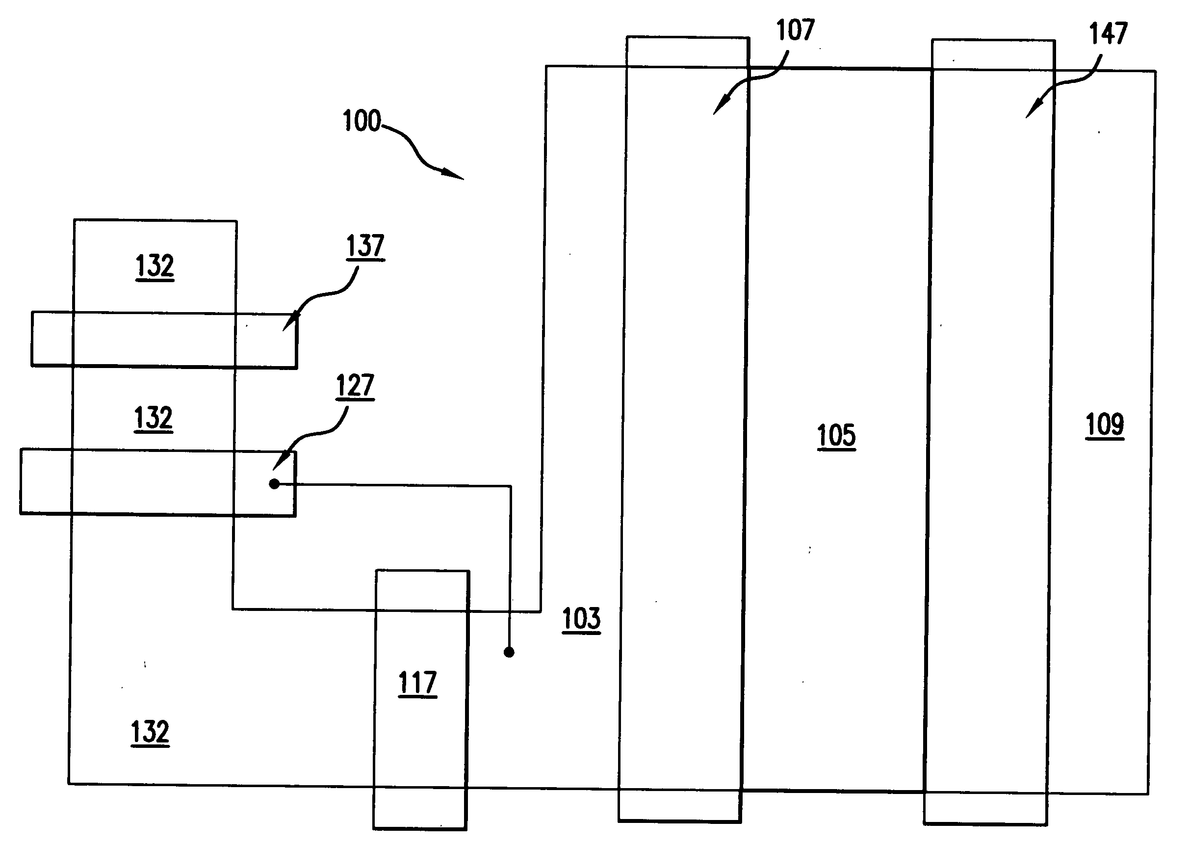
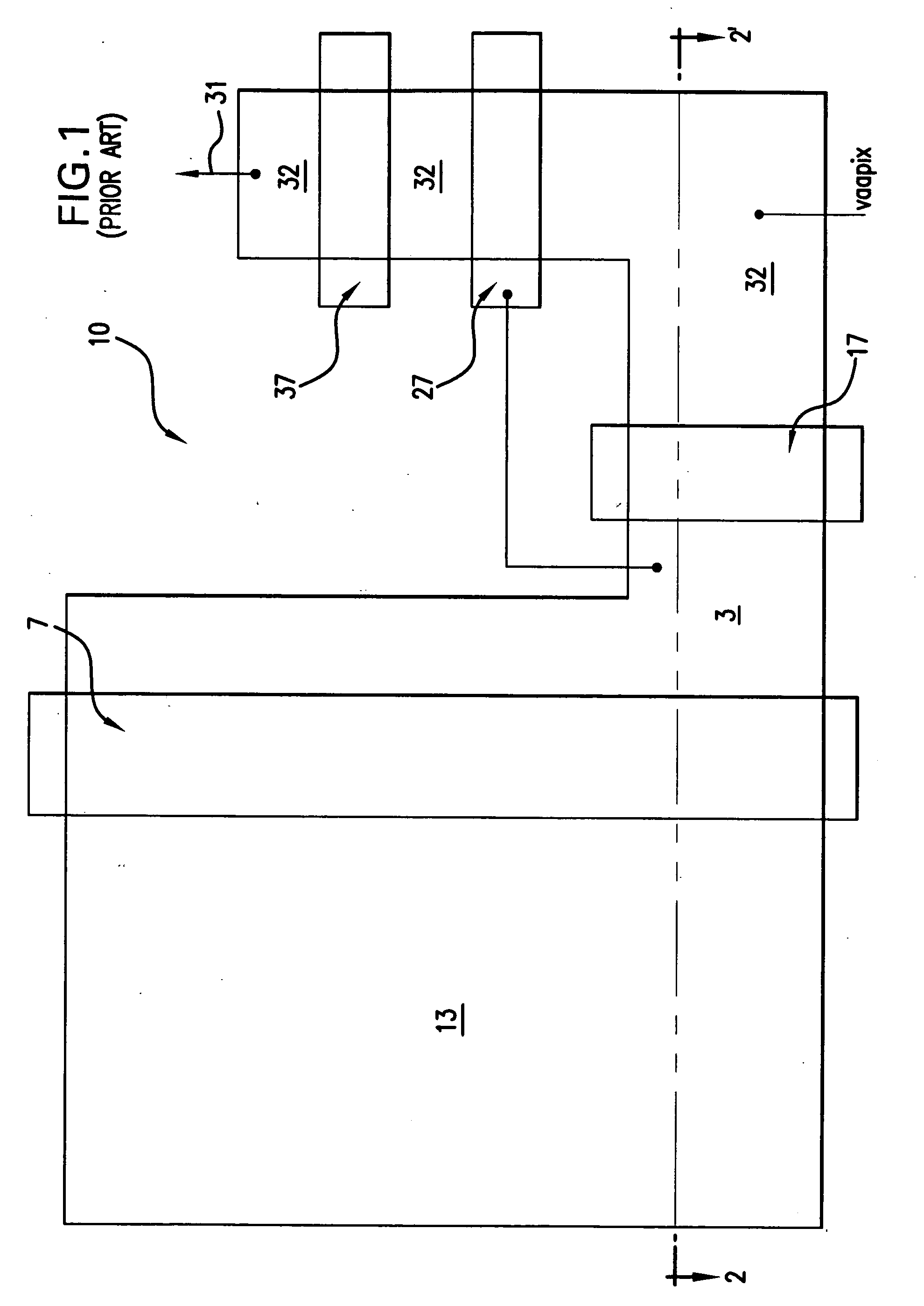
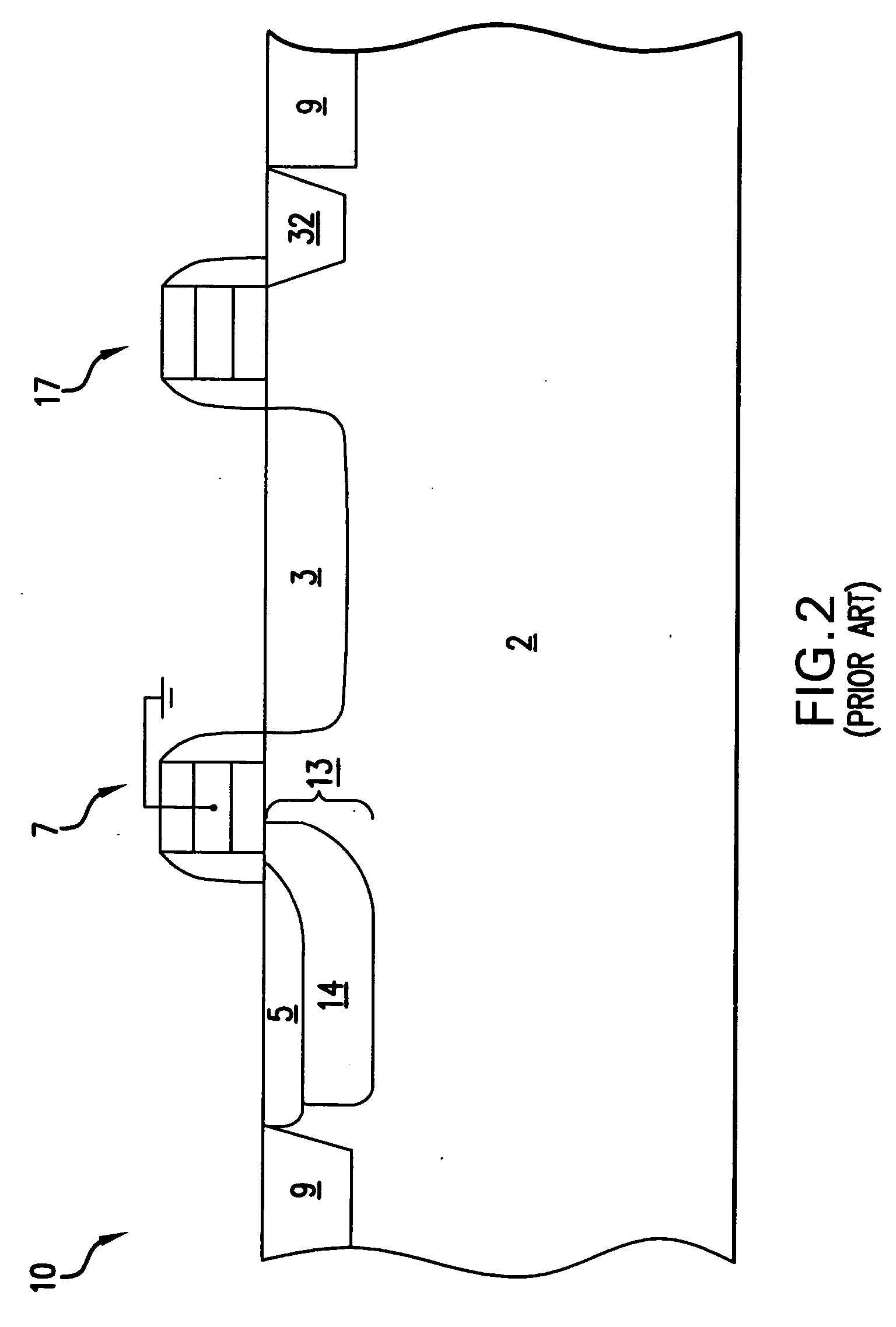
[0027] The term “pixel” or “pixel cell” refers to a picture element unit cell containing a photosensor (i.e., a photodiode) and transistors for converting electromagnetic radiation to an electrical signal. For purposes of illustration, a portion of a representative pixel cell is illustrated in the figures and description herein. Where methods of operation are described,...


PUM


Abstract

Methods for operating a pixel cell include efficient transferring of photo-charges using multiple pulses to a transistor transfer gate during a charge integration period for an associated photosensor. The pixel cell can be operated with efficient transfer characteristics in either normal or high dynamic range (HDR) mode. The high dynamic range can be realized by either operating an optional HDR transistor or by fluctuating the voltage applied to a reset gate.

Description

FIELD OF THE INVENTION [0001] The present invention relates generally to semiconductor devices, and more particularly, to transfer transistor technology, for use in imager pixels. BACKGROUND OF THE INVENTION [0002] CMOS image sensors are increasingly being used as low cost imaging devices. A CMOS image sensor circuit includes a focal plane array of pixel cells, each one of the cells includes a photosensor, such as e.g., a photogate, photoconductor, or photosensor having an associated charge accumulation region within a substrate for accumulating photo-generated charge. Each pixel cell may include a transistor for transferring charge from the charge accumulation region to a sensing node, and a transistor for resetting the sensing node to a predetermined charge level prior to charge transference. The pixel cell may also include a source follower transistor for receiving and amplifying charge from the sensing node and an access transistor, for controlling the readout of the cell conten...

Claims


Application Information

Patent Timeline
Patent Type & Authority Applications(United States)
IPC IPC(8): H01L31/062H04N5/355H04N5/374
CPCH01L27/14609H01L27/14654H04N5/235H04N5/374H04N5/3591H04N5/361H04N5/2355H04N23/70H04N23/741H04N25/575H04N25/621H04N25/63H04N25/76H04N25/57
Inventor MAURITZSON, RICHARD A.AGRANOV, GENNADIY A.HONG, SUNGKWON C.HONG, CANAAN S.
Owner APTINA IMAGING CORP
Why Eureka
Try Eureka