Nanoelectronic sensor with integral suspended micro-heater

a technology of nanotube sensors and micro-heaters, which is applied in the field of nanoelectronic sensors with integral suspended micro-heaters, can solve the problems of time-consuming and laborious, and achieve the effects of improving the responsiveness of nanotube sensors to hydrogen and other materials, accelerating the response, and improving the responsiveness of nanotube sensors

Inactive Publication Date: 2007-03-01
NANOMIX
View PDF2 Cites 64 Cited by
  • Summary
  • Abstract
  • Description
  • Claims
  • Application Information

AI Technical Summary

Benefits of technology

[0014] Such a nanotube device has demonstrated improved responsiveness to hydrogen and other materials. Surprisingly, it was found that the responsiveness of a nanotube sensor may be greatly enhanced by heating the nanotube independently of the substrate to which it is attached. This may be accomplished, for example, by ohmic heating. The device substrate may have a temperature substantially less than the heated nanostructure element (e.g., carbon nanotubes). For example, the base substrate may have a bulk temperature of less than about 100° C., where the operating temperature of the nanostructures (e.g., nanotube or nanotubes) attached to the substrate have a temperature substantially greater than 100° C., such as, for example, about 300° C. When operated in this condition, a nanotube sensor exhibits a much faster response to sensor targets such as hydrogen.
[0015] In alternative embodiments, the sensing device includes a platform or membrane which is at least partially thermally isolated by one or more cavities, the platform supporting at least the nanostructure element adjacent to a microheater element. The heating of the sensor structure may be employed, for example, for thermoregulation, to accelerate and / or increase sensor response, and to improve other sensor characteristics.

Problems solved by technology

Such response may deteriorate with time.

Method used


Image

  • Nanoelectronic sensor with integral suspended micro-heater
  • Nanoelectronic sensor with integral suspended micro-heater
  • Nanoelectronic sensor with integral suspended micro-heater

Examples


embodiment 40

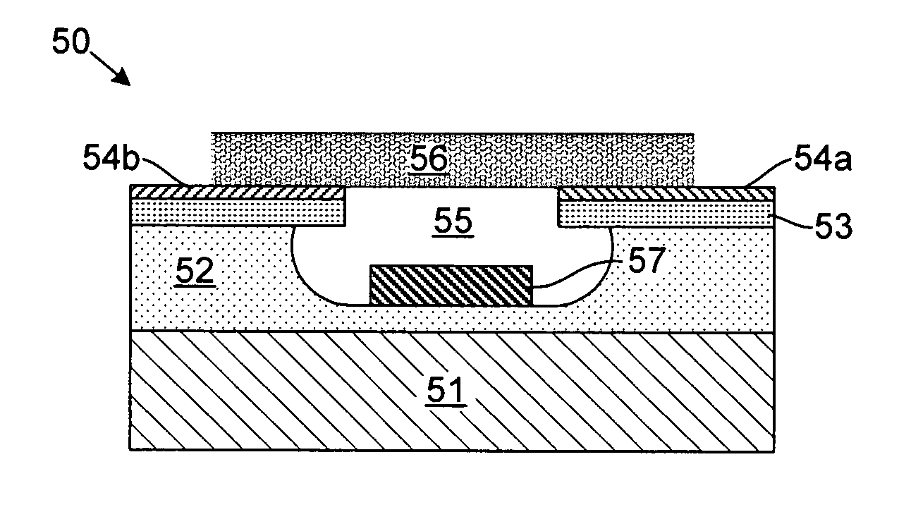
[0068]FIGS. 4.1-4.8 illustrate the structure of a sensor device embodiment 40 having aspects of the invention and including an exemplary micro-hotplate. For purposes of clarity in describing the physical relationship of the various elements of device 40, the exemplary process steps shown in FIGS. 4.1-4.8 will be discussed first. The exemplary fabrication processes shown are generally similar to those described in U.S. Pat. No. 6,894,359 entitled “Sensitivity Control For Nanotube Sensors”, which is incorporated by reference.

[0069] It should be understood, however, that the process steps shown in the figures are only examples, and that the technology of the electronics industry and related materials science, and in particular the technology of the MEMS, micro-machining and wafer processing industries provide a wide variety of process and materials alternatives which may be employed in making structures such as that of device 50, without undue experimentation and without departing from...

embodiment 60

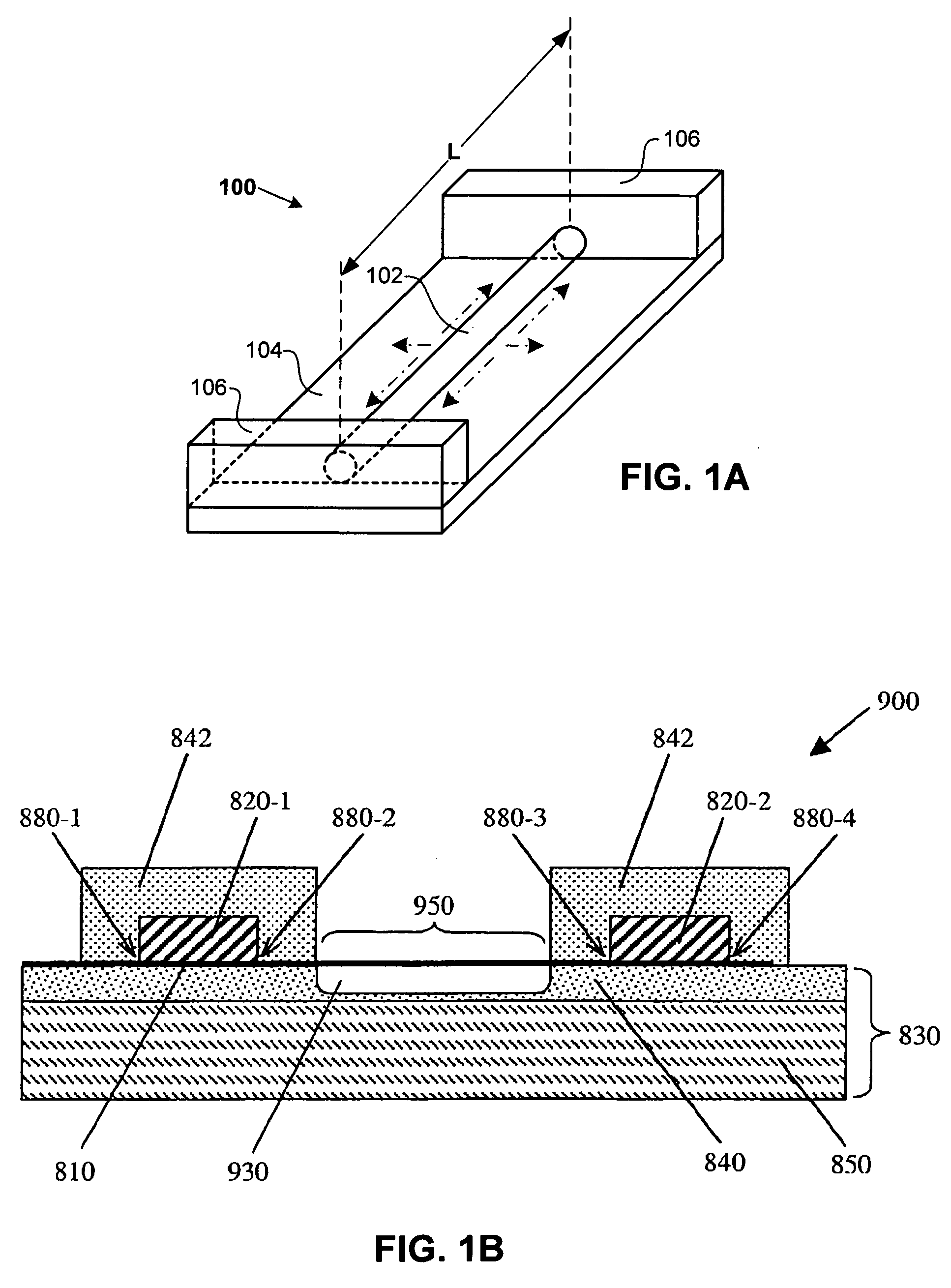
[0091]FIGS. 6.1-6.10 shows an alternative sequence of exemplary steps which may be employed for making the sensor device embodiment 60 having aspects of the invention. The fabrication processes shown make use of the differential in etch rate of porous silicon versus a crystalline silicon substrate, of the general nature of the processes described in US Published Application 2004-0195,096; and C. Tsamis et al, Physica Status Solidi (a), Vol. 197 (2), p. 539-543 (2003); as well as G. Kaltsas et al, “Front-side bulk silicon micromachining using porous silicon technology”, Sensors and Actuators: A, 65, (1998) p.175-179; and G. Kaltsas et al, “Bulk silicon micromachining using porous silicon sacrificial layers”, Microelec. Eng. 35, (1997), pp. 397-400, each of which are incorporated by reference.

[0092]FIG. 6.1 is a cross section showing the initial substrate 61 of device 60, in this example a doped monocrystalline silicon wafer.

[0093]FIG. 6.2 is a cross section showing the a pattern reg...


PUM


Abstract

A nanoelectronic sensing device includes a substrate, a nanostructure element disposed adjacent the substrate, and at least a conductive element electrically connected to the nanostructure element. The device is configured to heat at least a portion of the sensor structure including the nanostructure element. In certain embodiments, the nanostructure element comprises at least one nanotube, the nanotube being electrically connected to at least two conductors so as to permit an electric current on the order of 10 microAmps or greater to be passed through the nanotube, causing the nanotube to heat up relative to the substrate. In alternative embodiments, the sensing device includes a platform or membrane which is at least partially thermally isolated by one or more cavities, the platform supporting at least the nanostructure element adjacent to a microheater element. The heating of the sensor structure may be employed, for example, for thermoregulation, to accelerate and/or increase sensor response, and to improve other sensor characteristics.

Description

CROSS-REFERENCE TO RELATED APPLICATIONS [0001] This application is a continuation-in-part of and claims priority to U.S. patent application Ser. No. 10 / 655,529 filed Sep. 4, 2003 entitled “Improved Sensor Device With Heated Nanostructure”, which claims priority to U.S. Provisional Application No. 60 / 408,362 filed Sep. 4, 2002; [0002] This application is a continuation-in-part of and claims priority to U.S. patent application Ser. No. 10 / 280,265 filed Oct. 26, 2002 entitled “Sensitivity Control For Nanotube Sensors” (now U.S. Pat. No. 6,894,359), which claims priority to U.S. Provisional Application No. 60 / 408,412 filed Sep. 4, 2002; [0003] This application claims priority to US Provisional Application No. 60 / 700,953 filed Jul. 19, 2005 entitled “Improved Sensor Device With Heated Nanostructure, Including Sensor Having Thermally Isolated Nanostructure Element And Integrated Micro-Heater”. [0004] Each of the above identified patent applications are specifically incorporated herein, in...

Claims


Application Information

Patent Timeline
Patent Type & Authority Applications(United States)
IPC IPC(8): H01L29/82
CPCB82Y10/00G01K2211/00G01K5/486B82Y15/00
Inventor CHANG, YING-LANGABRIEL, JEAN-CHRISTOPHE P.SKARUPO, SERGEISTAR, ALEXANDERVALCKE, CHRISTIANWANG, QIAN
Owner NANOMIX
Why Eureka
Try Eureka