Semiconductor device and power conversion apparatus using the same

a technology of semiconductor and power conversion apparatus, applied in the direction of semiconductor/solid-state device details, electrical apparatus construction details, printed circuit board receptacles, etc., can solve the problems of power semiconductor circuit elements not having the layout that takes into account, inverter going into overload state, and heat generated locally in semiconductors

Active Publication Date: 2007-03-08
HITACHI LTD
View PDF1 Cites 39 Cited by
  • Summary
  • Abstract
  • Description
  • Claims
  • Application Information

AI Technical Summary

Benefits of technology

[0017] According to this invention, it is possible to provide a semiconduct

Problems solved by technology

However, the above-noted prior art approaches suffer from a problem that the heat generated is locally concentrated within semiconductor devices depending upon an operation state of power converter because of the fact that the positive side semiconductor circuit elements are disposed while being organized into a group whereas the negative semiconductor elem

Method used


Image

  • Semiconductor device and power conversion apparatus using the same
  • Semiconductor device and power conversion apparatus using the same
  • Semiconductor device and power conversion apparatus using the same

Examples


embodiment 1

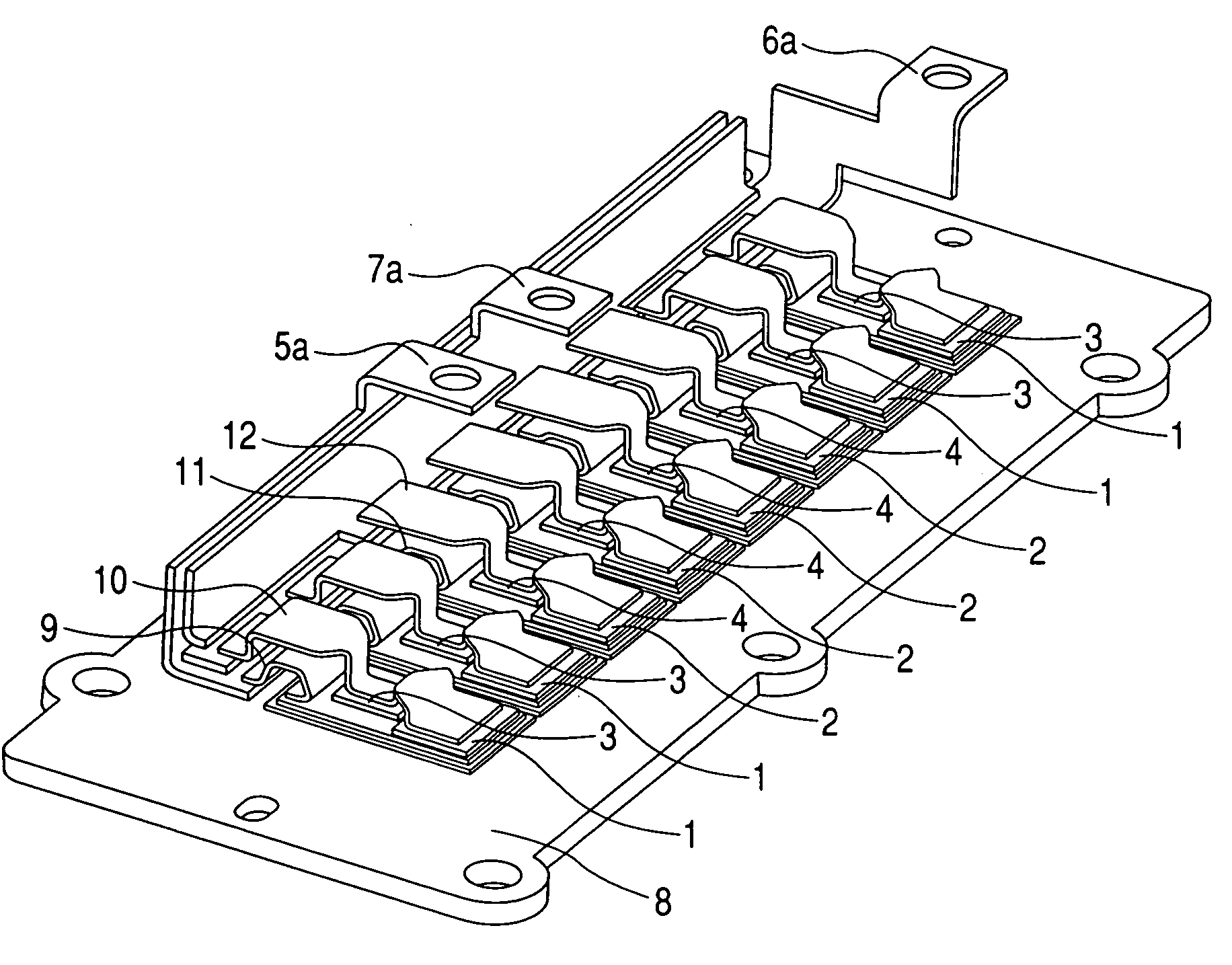
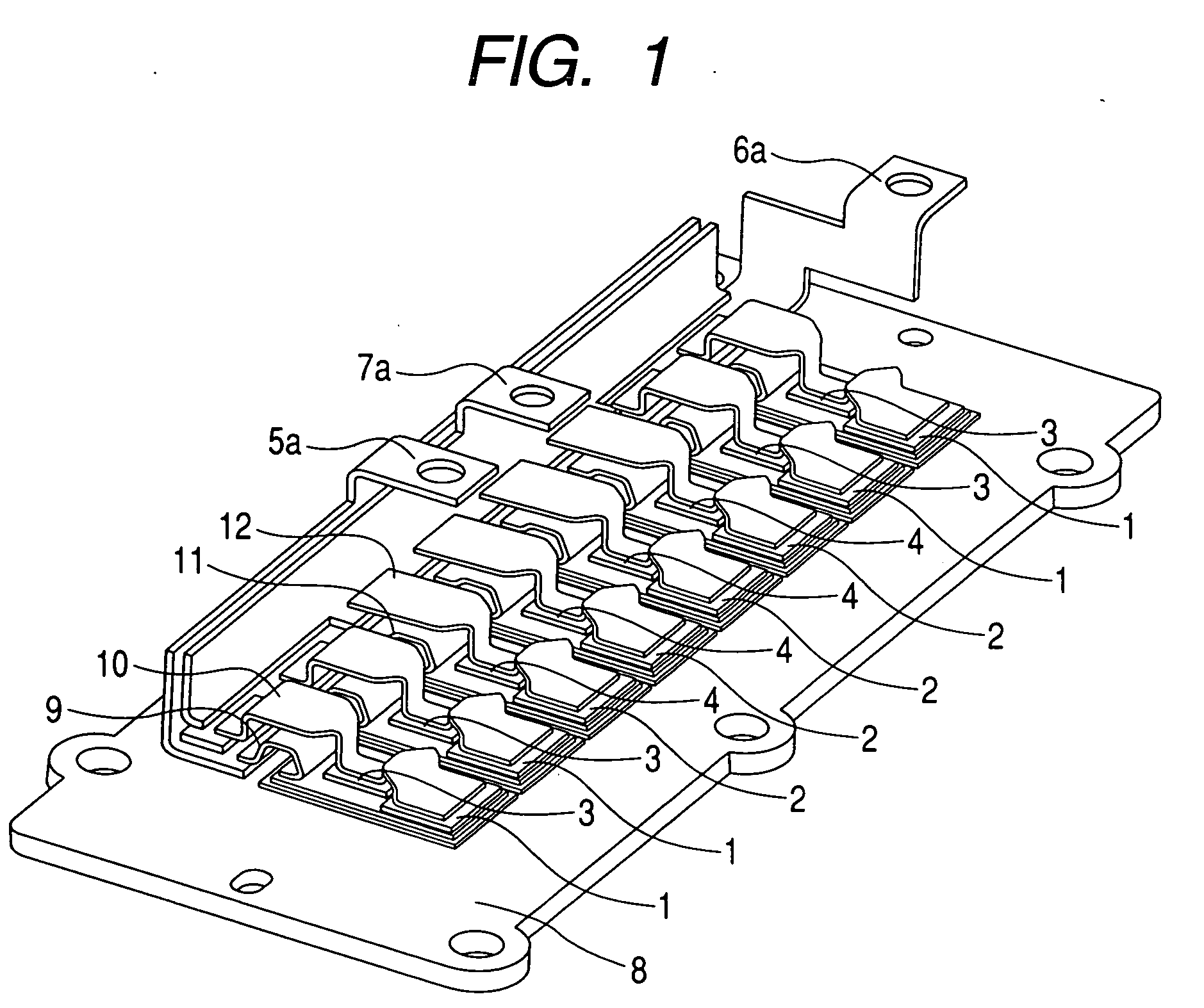
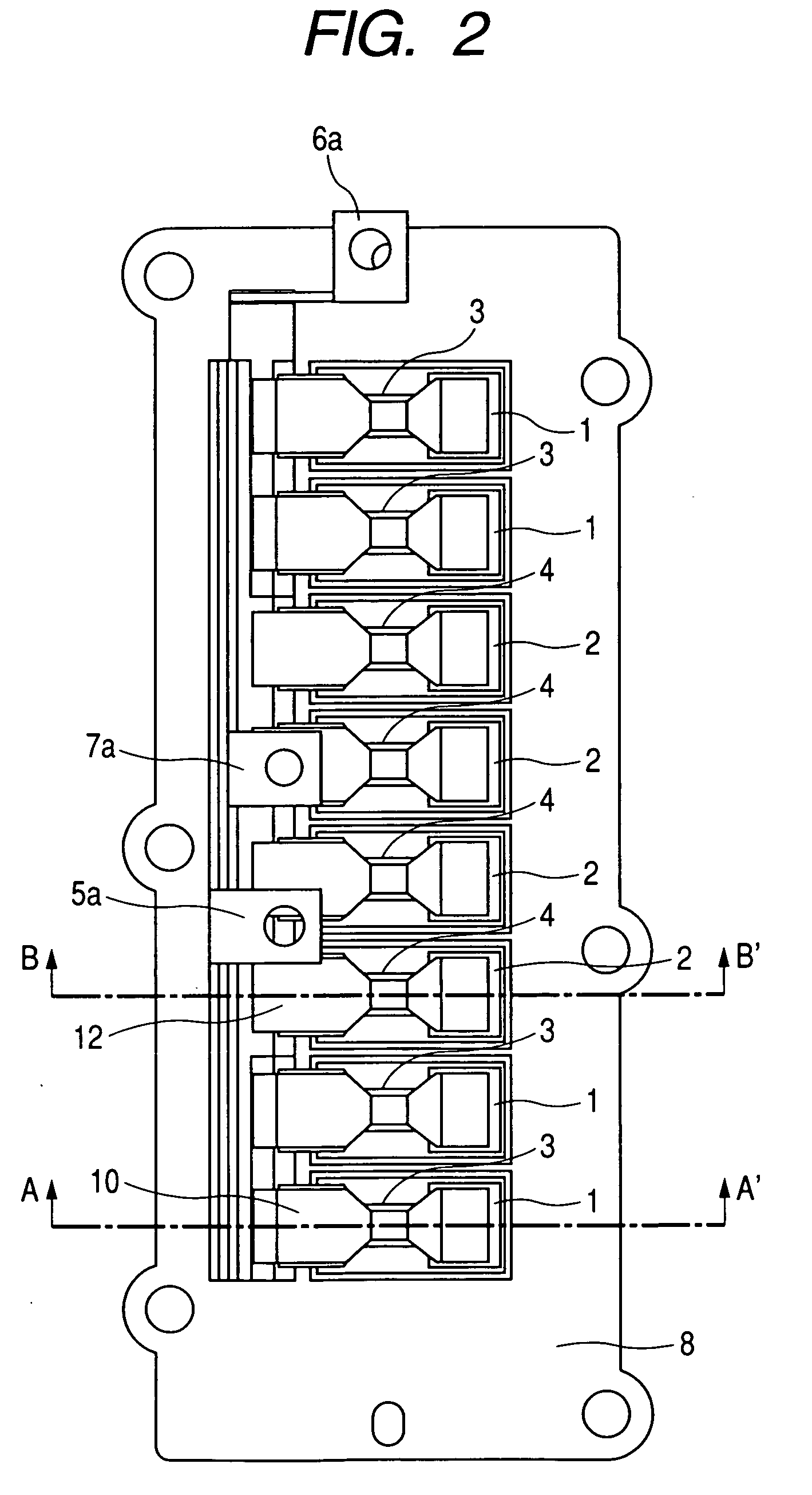
[0044] A configuration and operation of a semiconductor device in accordance with a first embodiment of this invention will be set forth while referring to FIGS. 1 to 4 and FIGS. 21 and 22.

[0045] An explanation will first be given of a circuit configuration for inductance reduction. See FIG. 21, which is a circuit diagram of a power conversion apparatus as connected to a DC power supply and a load. Shown herein is a case where the power converter circuitry includes switching power semiconductor circuit elements, e.g., insulated-gate bipolar transistors (IGBTs). Also note that several inductance components are illustrated in the circuit diagram for the purpose of considering electrical currents flowing during switching operations.

[0046] A power conversion apparatus 30 is connected to DC power supply 16 by inductance components 18 and 19 of a cable. Based on a command from a control device (not shown), an IGBT 1 of upper arm and an IGBT 2 of lower arm perform switching operations, w...

embodiment 2

[0064] A configuration and operation of a semiconductor device in accordance with a second embodiment of the invention will be described with reference to FIGS. 5 to 8. A perspective view of the semiconductor device 29 is shown in FIG. 5, which uses a group of four high voltage side circuit elements (IGBTs 1) and a group of four low voltage side circuit elements (IGBTs 2). A top view of the device is depicted in FIG. 6. Its high voltage side (positive polarity side) and low voltage side (negative polarity side) cross-sections are shown in FIGS. 7 and 8, respectively.

[0065] The embodiment shown herein is different from the first embodiment in that the high voltage side (positive side) and low voltage side (negative side) semiconductor circuit element groups are divided with a single power semiconductor element being as a unit while letting low voltage side power semiconductor elements (IGBTs 1 and 2) be disposed alternately.

[0066] A circuit diagram of this parts-mount structure is ...

embodiment 3

[0068] An explanation will next be given of a configuration and operation of a semiconductor device in accordance with a third embodiment of the invention with reference to FIGS. 9 to 12. A perspective view of the semiconductor device 29 is shown in FIG. 9, which uses a group of four high voltage side circuit elements (IGBTs 1) and a group of four low voltage side circuit elements (IGBTs 2). A top view of the device is depicted in FIG. 10. High voltage side (positive side) and low voltage side (negative side) cross-sections of it are shown in FIGS. 11 and 12, respectively.

[0069] This embodiment device is different from the first and second embodiments in that the high voltage (positive) side and low voltage (negative) side power semiconductor circuit elements (IGBTs 1-2) are divisionally organized into more than two—e.g., four—groups of semiconductor circuit elements, which are disposed in a couple of linear arrays so that a positive side conductive plate 5 and an output conductive...


PUM


Abstract

The power conversion apparatus uses the semiconductor device. Said semiconductor device includes a first group of power semiconductor elements at least one of which is electrically connected between a first potential and a third potential, a second group of power semiconductor elements at least one of which is electrically connected between a second potential and the third potential, and a third group of power semiconductor elements at least one of which is electrically connected between the first potential and the third potential. The second group is disposed between the first group and third group. Thereby, a low-loss semiconductor device having both inductance reducibility and heat generation balancing capability and also an electric power conversion apparatus using the same is provided.

Description

CLAIM OF PRIORITY [0001] The present application claims priority from Japanese application serial no. 2005-245232, filed on Aug. 26, 2005, the content of which is hereby incorporated by reference into this application. FIELD OF THE INVENTION [0002] The present invention relates in general to semiconductor devices and electrical power conversion apparatus using the same, and more particularly to a semiconductor device of the low-loss heat dispersion type adaptable for use in movable bodies, such as land vehicles or else, and power conversion apparatus using this device. BACKGROUND OF THE INVENTION [0003] In recent years, development is advancing of development of switchable large-current power semiconductor circuit elements. A power conversion apparatus configured from a semiconductor device using the power elements is expected to offer the ability to efficiently supply electric power to a load, such as a motor or else. Accordingly, such apparatus is widely employed for the purpose o...

Claims


Application Information

Patent Timeline
IPC IPC(8): H01L31/111
CPCH01L24/40H01L24/41H01L2924/1305H01L2924/00014H01L2924/01087H01L2924/01023H01L2924/01006H01L24/45H01L25/072H01L2224/45124H01L2924/01013H01L2924/01015H01L2924/01027H01L2924/01033H01L2924/01074H01L2924/01082H01L2924/13055H01L2924/13091H01L2924/19041H01L2924/30107H05K7/1432H01L2924/01005H01L2224/48H01L2924/00H01L2224/40137H01L2224/40139H01L2224/32225H01L2224/40091H01L2224/83801H01L24/32H05K7/14329H01L2224/37099H01L2224/84H01L2224/73221
Inventor AZUMA, KATSUNORIMORITA, TOSHIAKIHOZOJI, HIROSHISUZUKI, KAZUHIROSATOH, TOSHIYAOTSUKA, OSAMU
Owner HITACHI LTD
Why Eureka
Try Eureka