

Alignment marks for polarized light lithography and method for use thereof
a technology of alignment marks and polarized light, applied in the direction of photomechanical devices, instruments, optics, etc., can solve the problems of improper alignment of wafers, inoperable integrated circuits, and useless wafers, and achieve the effect of simplifying alignment mark design and us
- Summary
- Abstract
- Description
- Claims
- Application Information
AI Technical Summary
Benefits of technology
Problems solved by technology
Method used
Image

Examples
Embodiment Construction
[0023] The making and using of the presently preferred embodiments are discussed in detail below. It should be appreciated, however, that the present invention provides many applicable inventive concepts that can be embodied in a wide variety of specific contexts. The specific embodiments discussed are merely illustrative of specific ways to make and use the invention, and do not limit the scope of the invention.
[0024] The present invention will be described with respect to preferred embodiments in a specific context, namely semiconductor fabrication using polarized light lithography, as well as tool and wafer alignment for use in the semiconductor fabrication. The invention may also be applied, however, to other semiconductor fabrication techniques involving lithography, including those using non-polarized light.
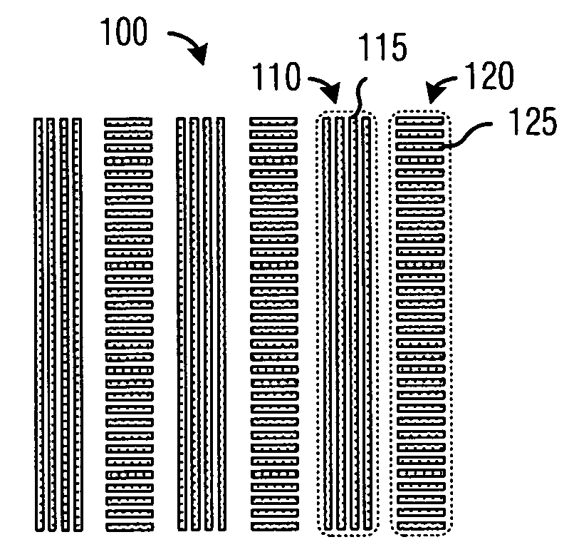
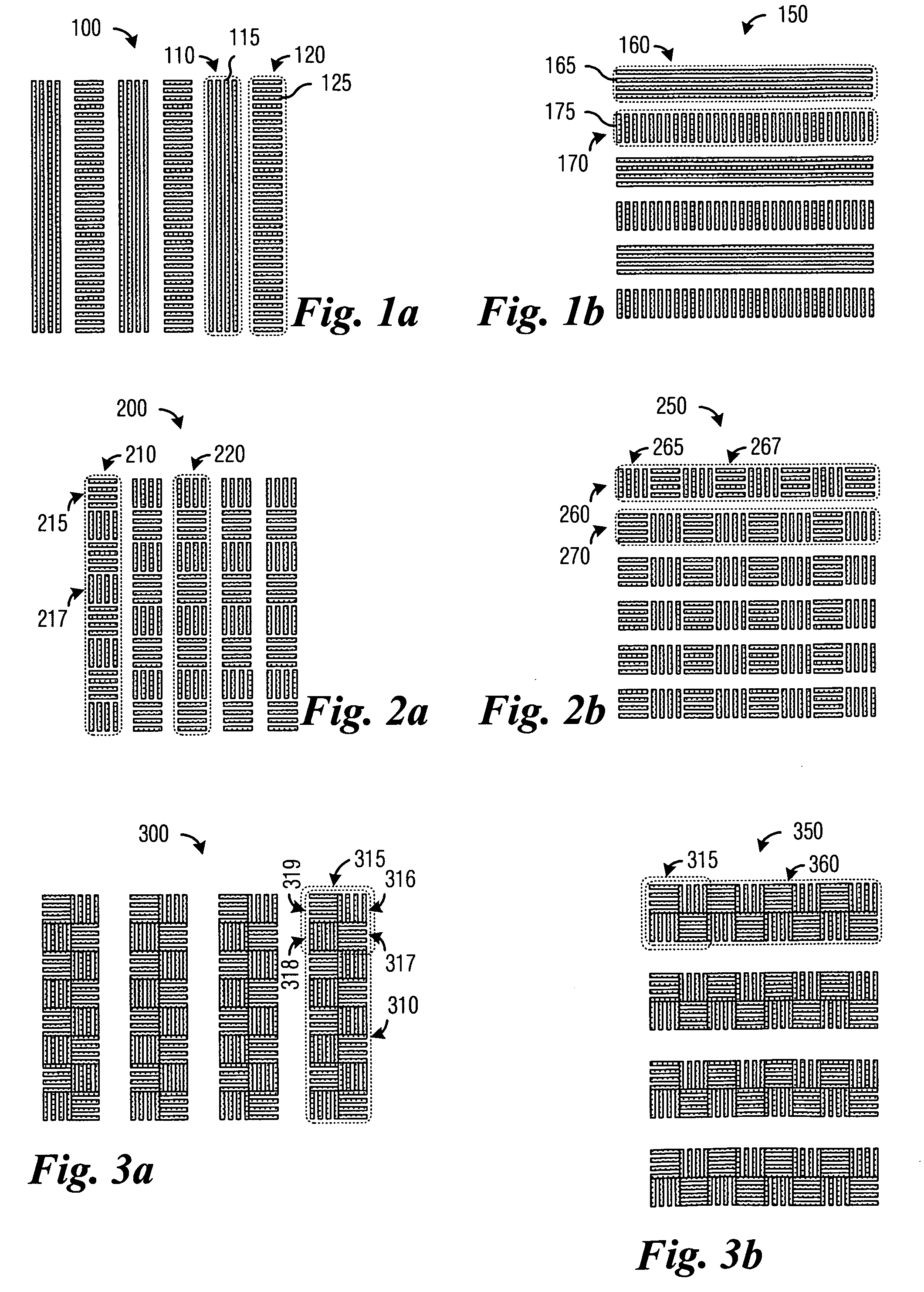
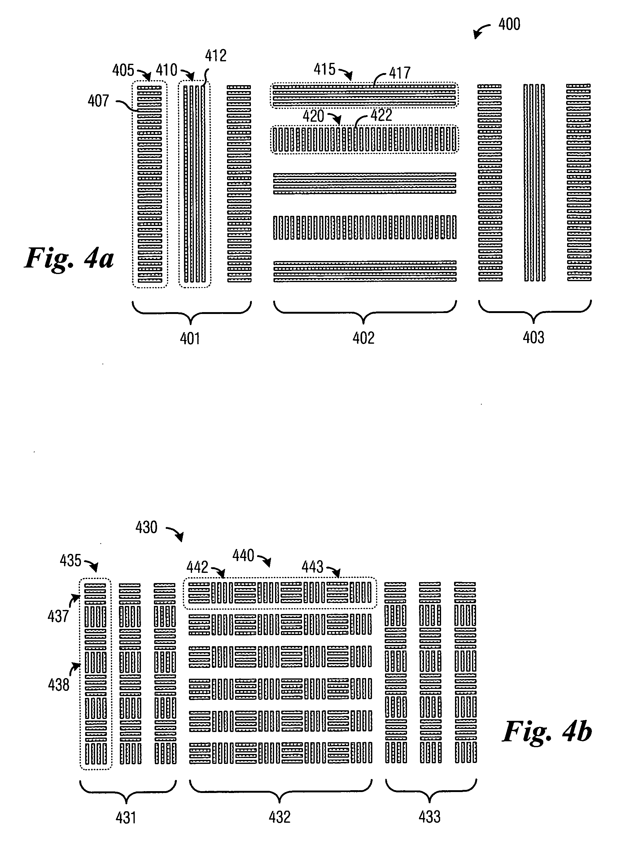
[0025] With reference now to FIGS. 1a and 1b, there are shown diagrams illustrating alignment marks for use in determining X-axis and Y-axis alignment, according to a pre...
PUM
 Abstract
Description
Claims
Application Information