Structure and fabrication of an MRAM cell

a technology of mram cells and mtjs, applied in the manufacture/treatment of galvano-magnetic devices, basic electric elements, electric devices, etc., can solve the problems of reducing the efficiency of bit line writing, thinning of oxide around the mtj stack, and increasing the cost of bit line to free layer distan

Inactive Publication Date: 2007-03-08
HEADWAY TECH INC
View PDF12 Cites 85 Cited by
  • Summary
  • Abstract
  • Description
  • Claims
  • Application Information

AI Technical Summary

Benefits of technology

[0012] Another object of at least one embodiment of the present invention has been to provide a capping layer for the MTJ that has minimal thickness, thereby minimizing the bit line to free layer distance and improving bit line writing efficiency.
[0013] Still another object of at least one embodiment of the present invention has been that said capping layer not be required to include a CMP stop layer.
[0014] A further object of at least one embodiment of the present invention has been to prevent MTJ deterioration caused by subsequent annealing.
[0015] A still further object of at least one embodiment of the present invention has been to provide a process that achieves the above objects without introducing substantial changes into existing methods for manufacturing MTJ based MRAM cells.

Problems solved by technology

There are two major problems associated with the conventional CMP process just described.
First, CMP usually leads to thinning of the oxide around the MTJ stack including the tunneling junction itself.
In some designs a very thick capping layer is used to prevent this kind of MTJ junction shorting, but this comes at the cost of increased bit line to free layer distance and reduced bit line writing efficiency.

Method used


Image

  • Structure and fabrication of an MRAM cell
  • Structure and fabrication of an MRAM cell
  • Structure and fabrication of an MRAM cell

Examples


Embodiment Construction

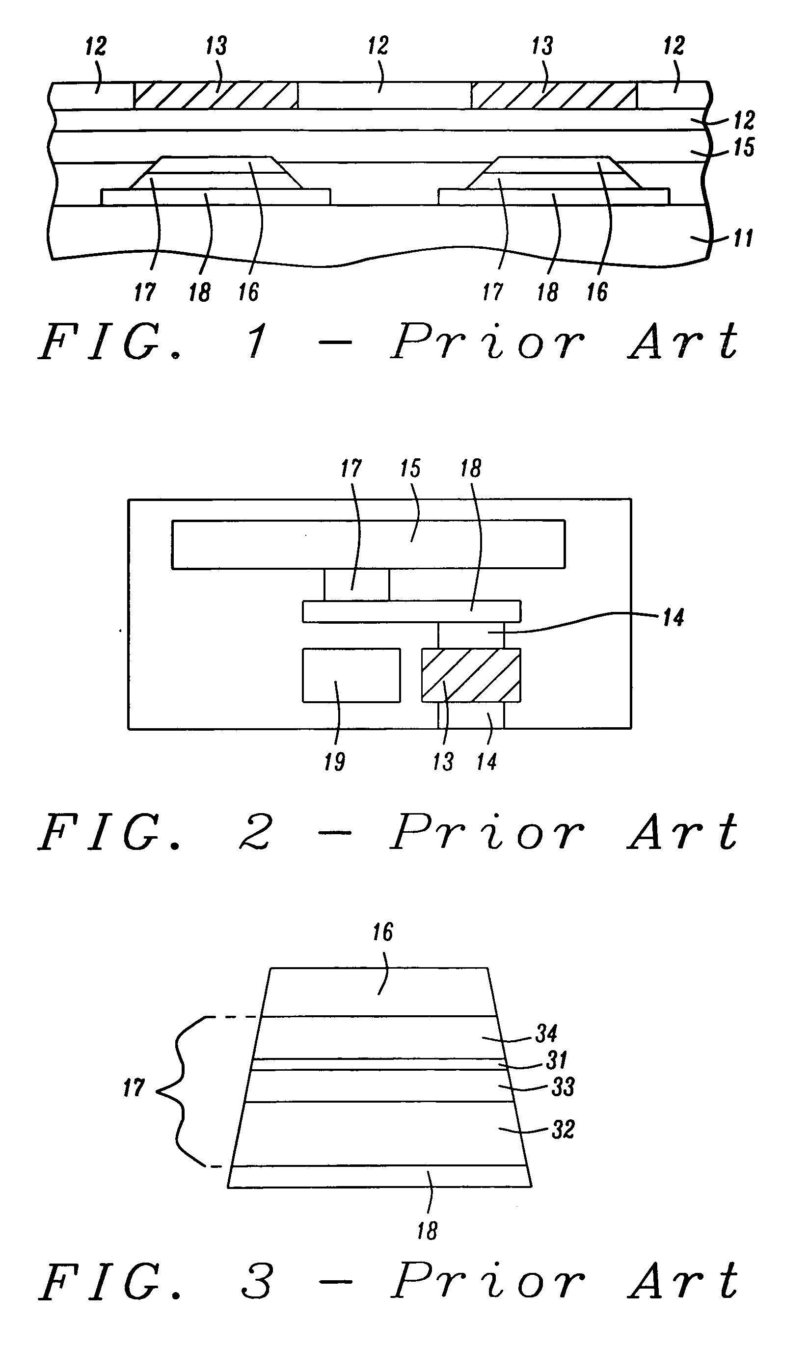
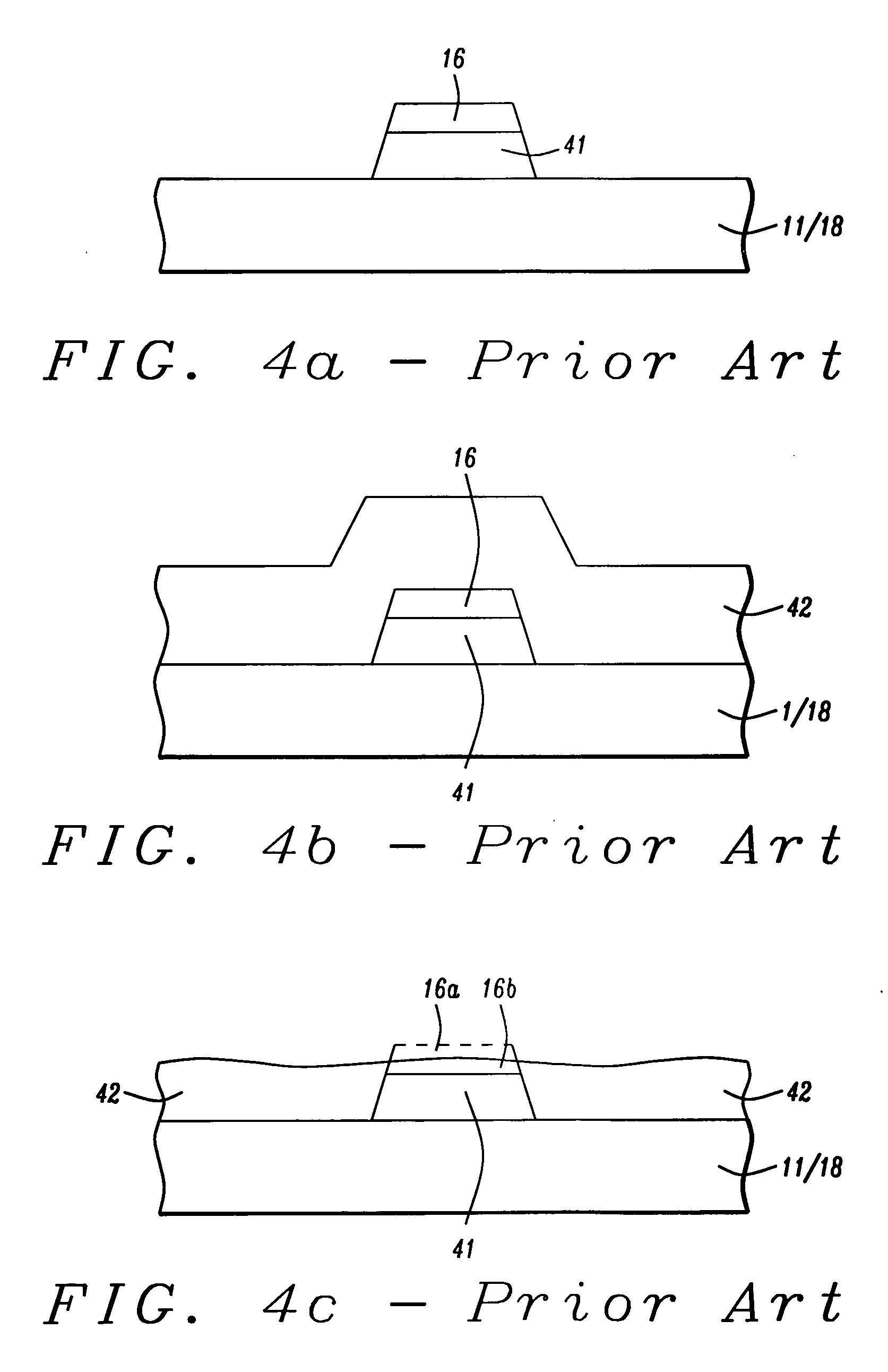
[0025] As noted earlier, in the prior art the exact stopping point for the CMP in the capping layer cannot be well controlled, varying from device to device and from wafer to wafer. As a result, control of the distance between the bit line and the free layer(s) is poor. Because the strength of the magnetic field generated by the bit line current at the free layer(s) depends strongly on the distance between the bit line and free layer(s), the inability to control this distance translates directly to the inability to control the switching magnetic field at the free layer(s), leading to degradation of device performance.

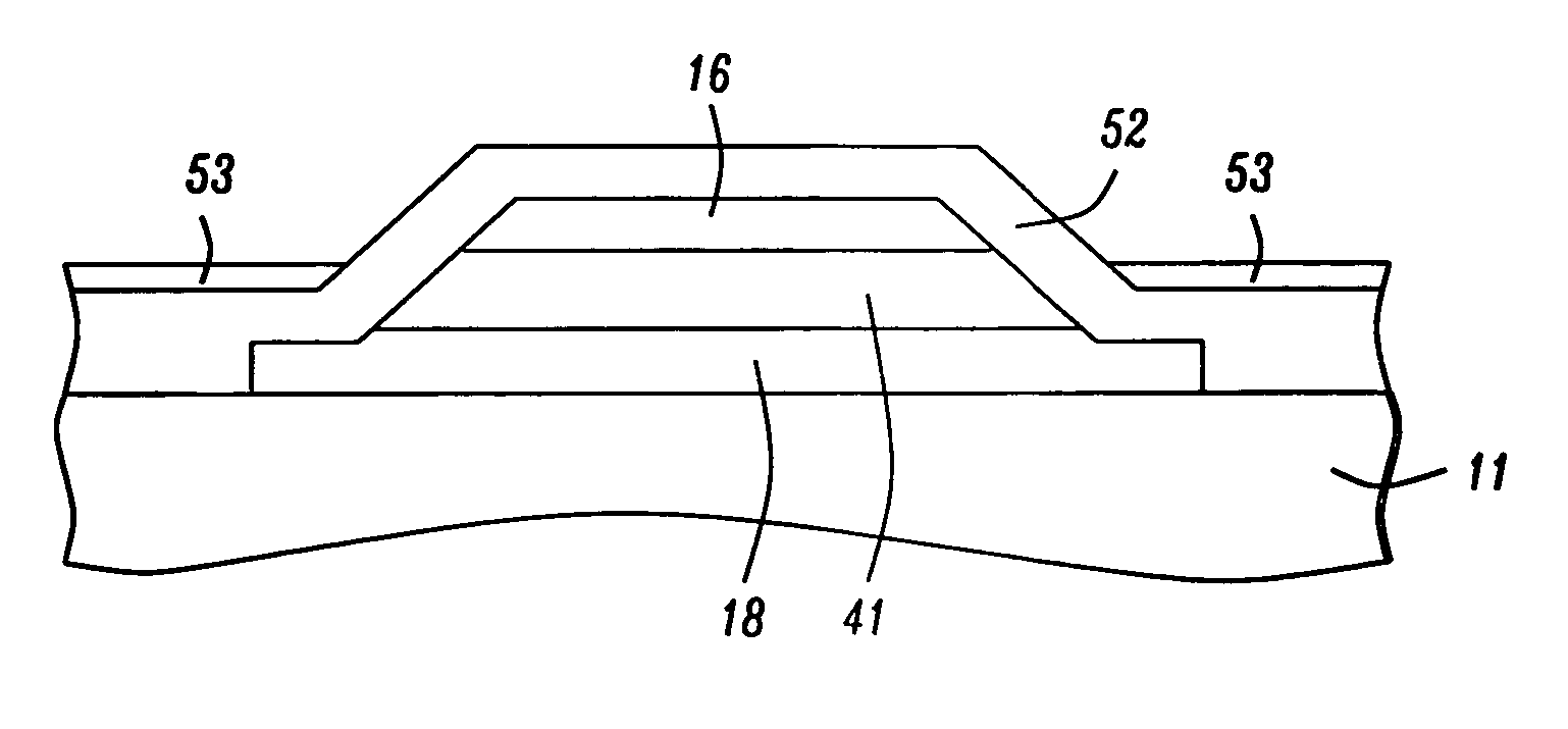
[0026] The present invention solves this problem through a new process to fabricate the MRAM chips that results in a MRAM cell structure with reduced MTJ shorting and a well controlled distance from bit line to free layers. In this process, a layer of silicon nitride or silicon oxynitride is deposited on the patterned MTJ junctions for extra protection, before the depo...


PUM


Abstract

MTJ stacks formed using prior art processes often fail because of shorts between the pinned layer and the top electrode. This problem has been overcome by depositing a protective layer on the MTJ sidewalls followed by an inter-layer dielectric. Then planarizing until the protective layer is just exposed. Finally, an etching (or second CMP) process is used to selectively remove the protective layer from the top surface of the cap layer.

Description

FIELD OF THE INVENTION [0001] The invention relates to the general field of magnetic random access memories (MRAMs) with particular reference to protecting magnetic tunnel junctions (MTJs). BACKGROUND OF THE INVENTION [0002] An MRAM chip consists of arrays of MRAM cells connected by bit lines and word lines. Each cell has at least one magnetic junction that is formed between at least two current carrying conductor lines. The magnetic junction of the cell stores information in the form of different magnetic states. FIG. 1 shows a cross-sectional view of two adjacent MRAM cells on common substrate 11. The three parts of the cell that are shown in FIG. 1 are bottom electrode 18, active region 17 (presented in greater detail in FIG. 3), and cap layer 16. Word lines are shown here as being above bit line 15 but may also be formed below bottom electrodes, as shown schematically in FIG. 2 as 19. Note that all regions labeled 12 represent insulation while the two regions labeled 14 represen...

Claims


Application Information

Patent Timeline
Patent Type & Authority Applications(United States)
IPC IPC(8): H01L21/336
CPCH01L43/12H10N50/01
Inventor HONG, LIUBOCHEN, MAO-MINMIN, TAICHEN, JUN
Owner HEADWAY TECH INC
Why Eureka
Try Eureka