Solid state imaging device and adjustment method thereof

a technology of solid state imaging and adjustment method, which is applied in the direction of color television details, television system details, television systems, etc., can solve the problem of variance in the signal output of the output amplifier unit, and achieve the effect of suppressing variance in the sensitivities of the output unit, reducing conversion efficiency, and high frame ra

Inactive Publication Date: 2007-03-15
SONY CORP
View PDF6 Cites 1 Cited by
  • Summary
  • Abstract
  • Description
  • Claims
  • Application Information

AI Technical Summary

Benefits of technology

[0028] Reference light is applied to the optical reception units, and the capacitance value of the variable capacitor is adjusted in accordance with a detection result of an electric signal output from each output unit. It is therefore possible to adjust the total capacitance associated with the charge/voltage conversion unit by adjusting the parasitic capacitance of the charge/voltage conversion unit,...

Problems solved by technology

However, as signal charges of one frame are output to a plurality of output amplifier units at...

Method used


Image

  • Solid state imaging device and adjustment method thereof
  • Solid state imaging device and adjustment method thereof
  • Solid state imaging device and adjustment method thereof

Examples


Embodiment Construction

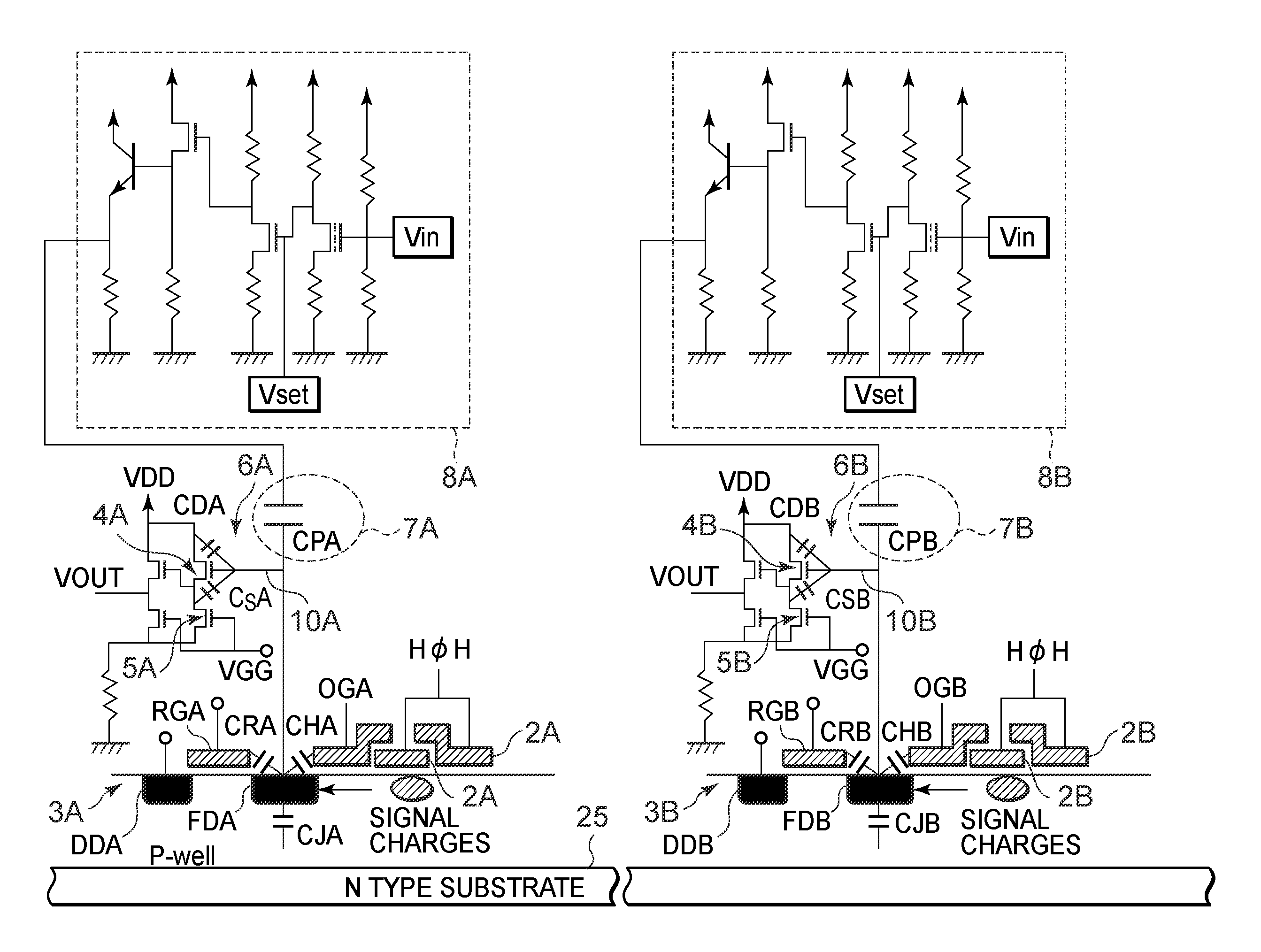
[0037] With reference to the accompanying drawings, an embodiment of the present invention will be described to help understand the present invention. The embodiment will be described by using as an example a solid state imaging device in which two horizontal transfer registers are provided and signal charges are output form two output amplifier units at the same time.

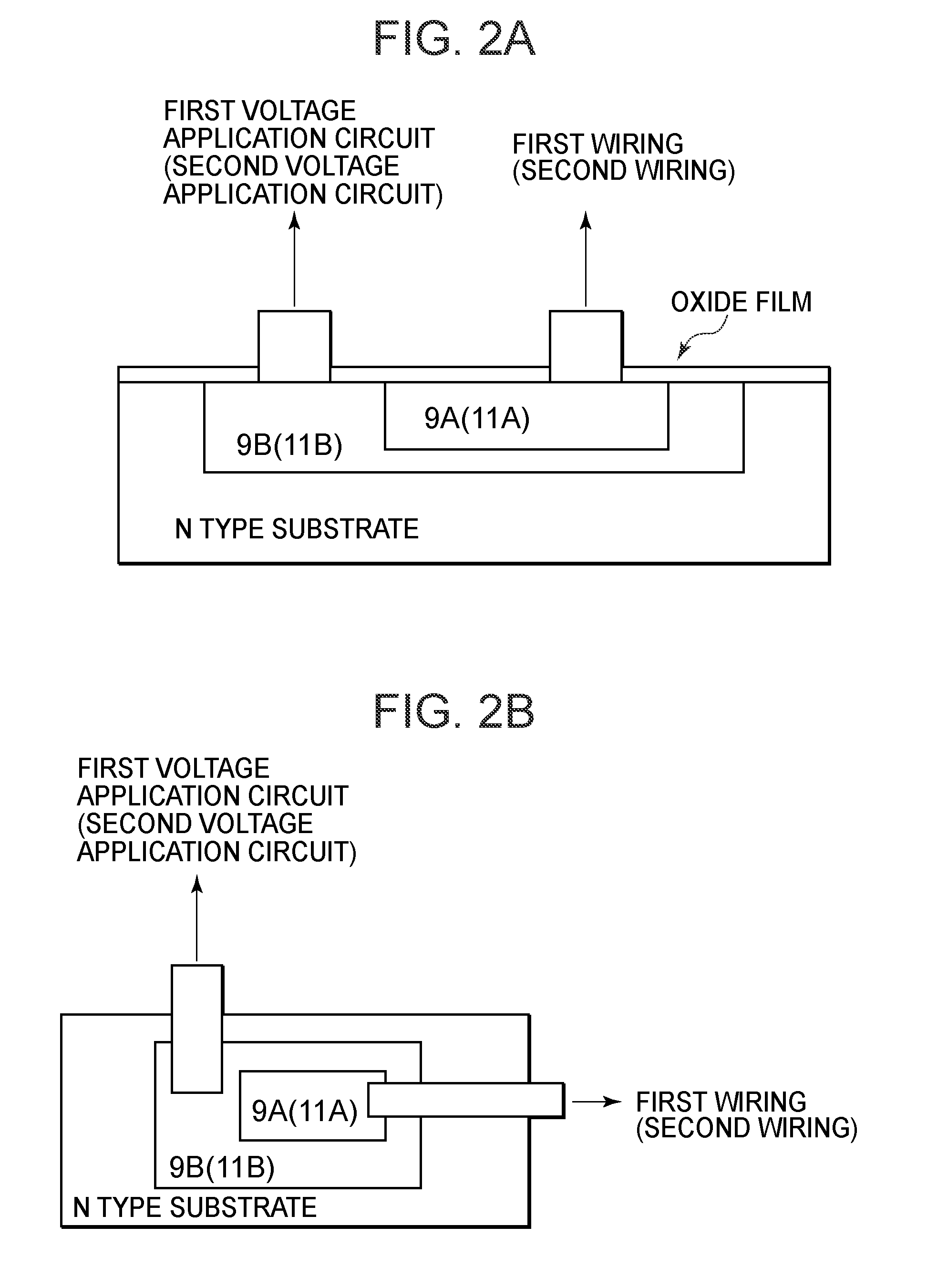
[0038]FIG. 1 is a schematic diagram showing an example of a solid state imaging device according to an embodiment of the present invention. The solid state imaging device shown in FIG. 1 has: at the next stages of horizontal transfer registers 2 (a first horizontal transfer register 2A and a second horizontal transfer register 2B) via output gates OG (a first output gate OGA and a second output gate OGB), discharge devices 3 (a first discharge device 3A and a second discharge device 3B) including floating diffusions FDs (a first floating diffusion FDA and a second floating diffusion FDB), reset gates RGs (a first rese...


PUM


Abstract

A solid state imaging device includes: two or more output units, the output unit including a charge/voltage conversion unit adapted to convert signal charges into an electric signal and an output circuit unit adapted to output the electric signal converted by the charge/voltage conversion unit; and a variable capacitor connected to a wiring, the wiring interconnecting the charge/voltage conversion unit and the output circuit unit.

Description

CROSS REFERENCES TO RELATED APPLICATIONS [0001] The present application claims the benefit of priority to Japanese Patent Application JP 2005-264988 filed in the Japanese Patent Office on Sep. 13, 2005, which is incorporated herein to the extent permitted by law. BACKGROUND OF THE INVENTION [0002] 1. Field of the Invention [0003] The present invention relates to a solid state imaging device and its adjustment method. More particularly, the present invention relates to a solid state imaging device having two or more charge / voltage conversion units and two or more output circuit units, and to its adjustment method. [0004] 2. Description of Related Art [0005] Video cameras and electronic cameras have been using a CCD type solid state imaging device having CCD registers as transfer registers (charge transfer units). [0006] In a CCD type solid state imaging device, a plurality of pixels having photoelectric conversion means (photodiodes: PDs) are disposed in an image area of a semiconduc...

Claims


Application Information

Patent Timeline
IPC IPC(8): H04N5/335H04N5/365H04N5/369H04N5/372H04N5/378
CPCH04N5/335H04N25/00
Inventor FUJITA, YUKIO
Owner SONY CORP
Why Eureka
Try Eureka