Method of linearizing ESD capacitance

a technology of esd capacitance and linearization, applied in the direction of pulse technique, transistor, electrical apparatus, etc., can solve the problems of circuits introducing load capacitance, circuits are susceptible to and may be destroyed, and produce destructive esd events, etc., and achieve the effect of positive negative voltage coefficient of drain capacitan

Inactive Publication Date: 2007-03-15
SEMICON COMPONENTS IND LLC
View PDF6 Cites 2 Cited by
  • Summary
  • Abstract
  • Description
  • Claims
  • Application Information

AI Technical Summary

Benefits of technology

[0011] The present invention provides an ESD protection circuit to both ground, Vss, and a power rail, Vcc. In a preferred embodiment, the protection device to ground is an NMOS with its drain connected to the pad being protected. An NMOS has a negative voltage coefficient of drain capacitance. In this embodiment, the protection device to the power rail is a PMOS with its drain connected to the pad. A PMOS has a positive voltage coefficient of drain capaci

Problems solved by technology

Integrated circuits are susceptible to and may be destroyed by ESD pulses.
But, other sources may produce destructive ESD events.
However, a limitation of the '258 circuit and other prior art ESD pr

Method used


Image

  • Method of linearizing ESD capacitance
  • Method of linearizing ESD capacitance
  • Method of linearizing ESD capacitance

Examples


Embodiment Construction

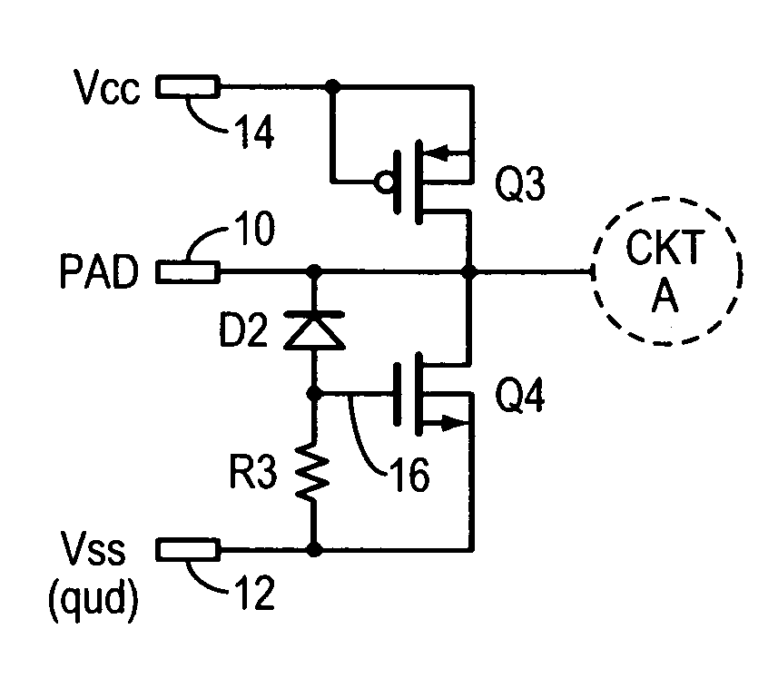
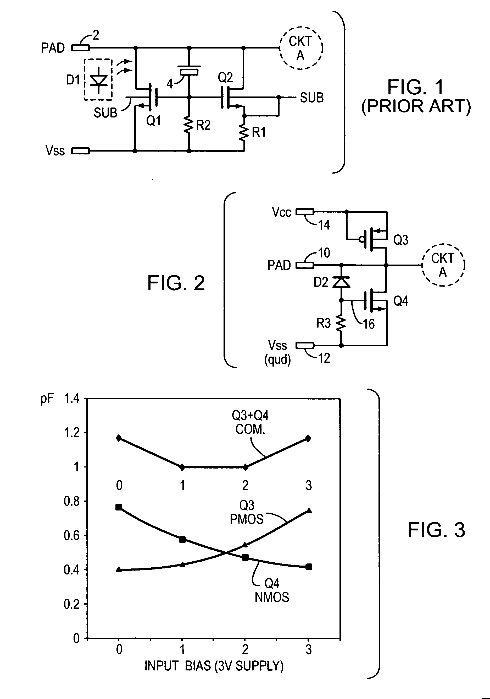
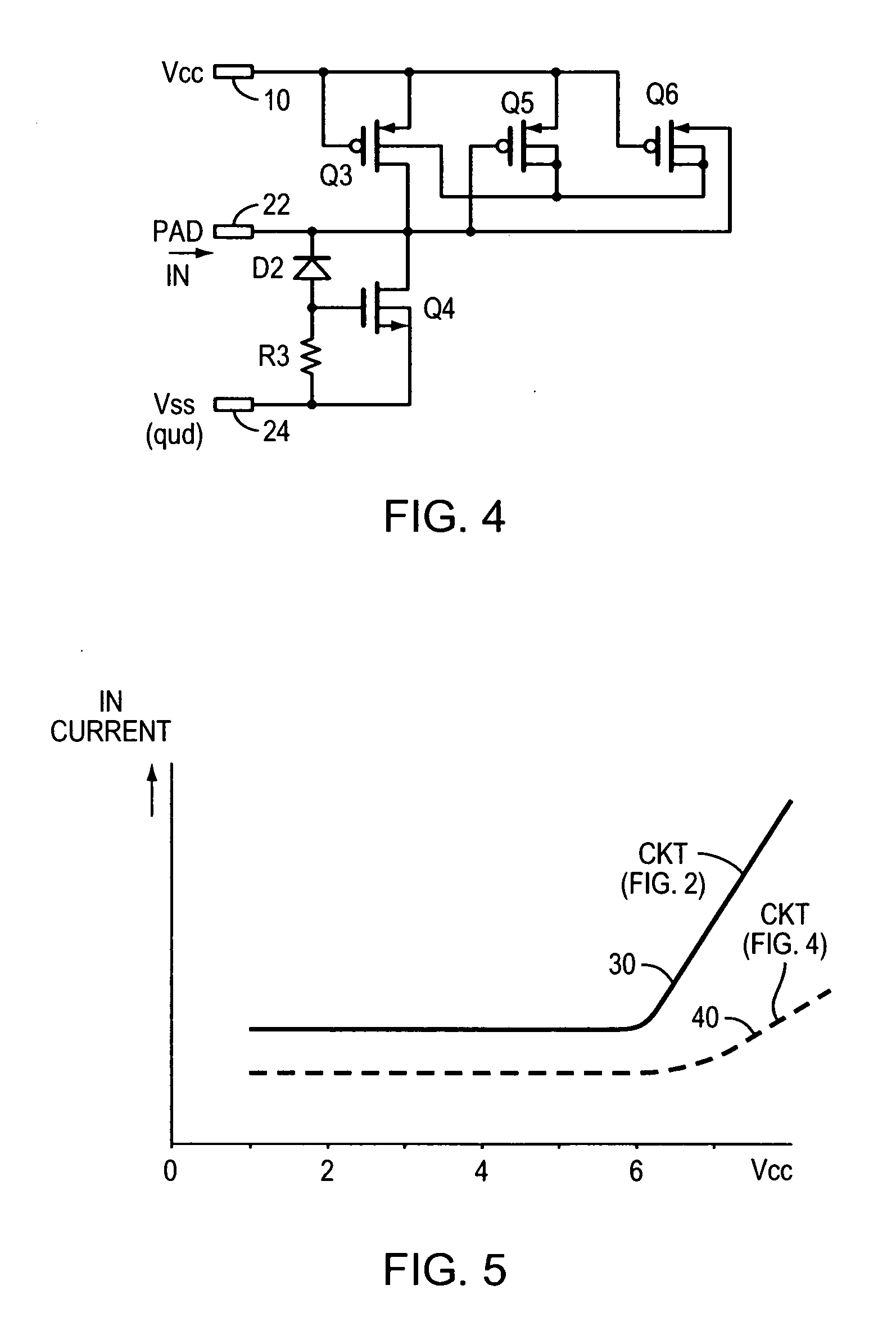
[0021]FIG. 2 illustrates a ESD protective circuit connected to the pad 10 for protecting the circuit CKT A from an ESD pulse that might appear on the pad. The approach is to dissipate or discharge the ESD pulse appearing at the pad 10 directly to ground 12 and / or Vcc 14 with little or no high voltage or current spikes entering CKT A. Importantly, concurrent with the ESD protection, the load capacitance of the protection circuit is made substantially constant with the input signal voltage on the pad 10.

[0022] With respect to ESD protection, the diode D2 is reverse biased establishing a capacitive path from the pad 10 to the gate 16 of Q4. A rising ESD pulse is coupled to the gate 16 turning on Q4 thereby discharging the ESD pulse. In another preferred embodiment, the techniques described and taught in the '066 and the '258 patents, where NMOS transistors share the same substrate and one drives the substrate whereby the second turns on more fully, may be implemented within the presen...


PUM


Abstract

An ESD protection circuit for an input/output pad of an IC is disclosed with discharge paths to both a power rail and ground. The ESD circuit is arranged with NMOS and PMOS transistors arranged with their drains connected to the pad. However, the drain capacitances have voltage sensitivities that compensate or cancel each other, and with proper sizing the capacitance load on the pad can be made substantially constant over a given voltage range. By providing a discharge path to a power rail, the ESD circuit may be designed to be more tolerant of overvoltages on the power rail.

Description

BACKGROUND OF THE INVENTION [0001] 1 Field of the Invention [0002] The present invention relates to electrostatic discharge (ESD) protection circuitry for an IC (integrated circuit) input, and more particularly to controlling the load capacitance of the protection circuitry on the input. [0003] 2 Background Information [0004] Integrated circuits are susceptible to and may be destroyed by ESD pulses. It is known that such ESD pulses may emanate from several sources, one primary source being from a human touching the IC. But, other sources may produce destructive ESD events. Such ESD pulses may include thousands of voltage and amperes of current that exist for a hundred nanoseconds or so. ESD events (defined as discharges or pulses) typically drive current into the IC, but may also sink current from the IC. Protection from both types is provided. [0005] Protection devices and circuits have been developed over a number of years that have provided reliable protection. Some of these prot...

Claims


Application Information

Patent Timeline
IPC IPC(8): H02H9/00
CPCH03K2217/0018H01L27/0266
Inventor MISKE, MYRONMORRILL, DAVID
Owner SEMICON COMPONENTS IND LLC
Why Eureka
Try Eureka