LED package

a technology of leds and packaging, applied in the field of led packages, can solve the problems of consuming massive power of leds, compromising the service life or leds, preventing related circuits from providing normal functions, etc., and achieves the effect of effective heat dissipation and much more flexibility

Inactive Publication Date: 2007-03-22
LEXTAR ELECTRONICS CORP
View PDF10 Cites 151 Cited by
  • Summary
  • Abstract
  • Description
  • Claims
  • Application Information

AI Technical Summary

Benefits of technology

[0007] The primary purpose of the present invention is to provide a simple structure secured on the heat slug for the connection between the LED and the lead frame to achieve effective heat dissipation purpose.
[0008] To achieve the purpose, the package of the present invention includes a heat slug to secure multiple LEDs, two lead frames with conducting area extending along the edge of the heat slug, and an encapsulating material constituting the connection between the heat slug and the lead frames. Multiple LED chips are connected to the conducting area by means of gold wire so to free each LED chip from the restriction imposed by the lead frames. Accordingly, the location of each LED chip may be deployed with much more flexibility.

Problems solved by technology

When functioning as a backlight source for a liquid crystal display (LCD) or a lighting fixture, the LED consumes massive power, and more waste heat is generated when multiple LEDs are lighted at the same time.
The waste heat from LEDs though is not at a temperature as high as that does by a tungsten filament lamp, it may prevent related circuits from providing normal functions or compromise the service life or the LEDs.
However, in either way, it is blamed for complicated manufacturing process, comparatively higher nonconformity rate, and difficulties in providing specific circuit for the circuit layout in coping with the location of the chip.

Method used


Image

  • LED package
  • LED package
  • LED package

Examples


Embodiment Construction

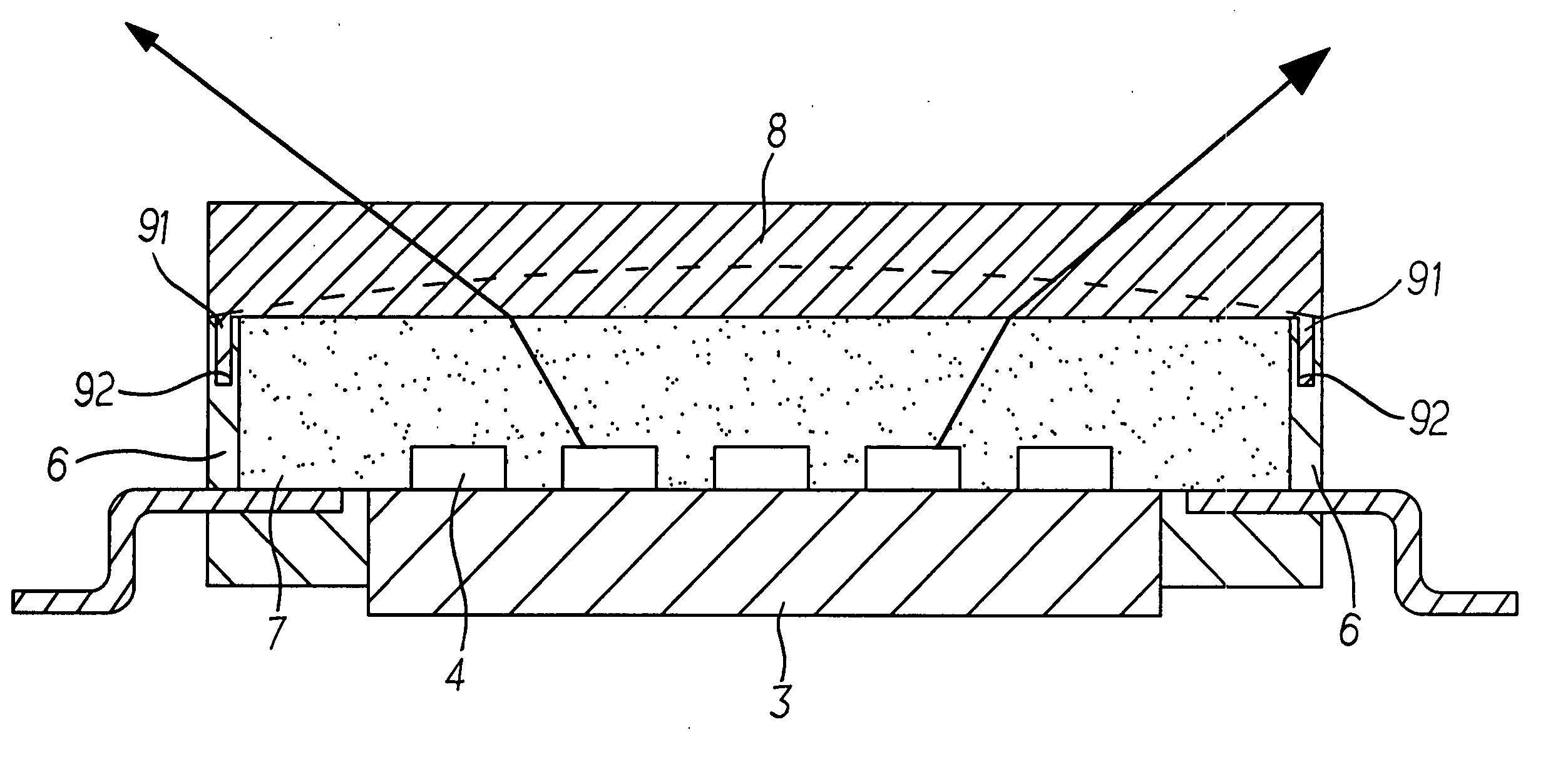
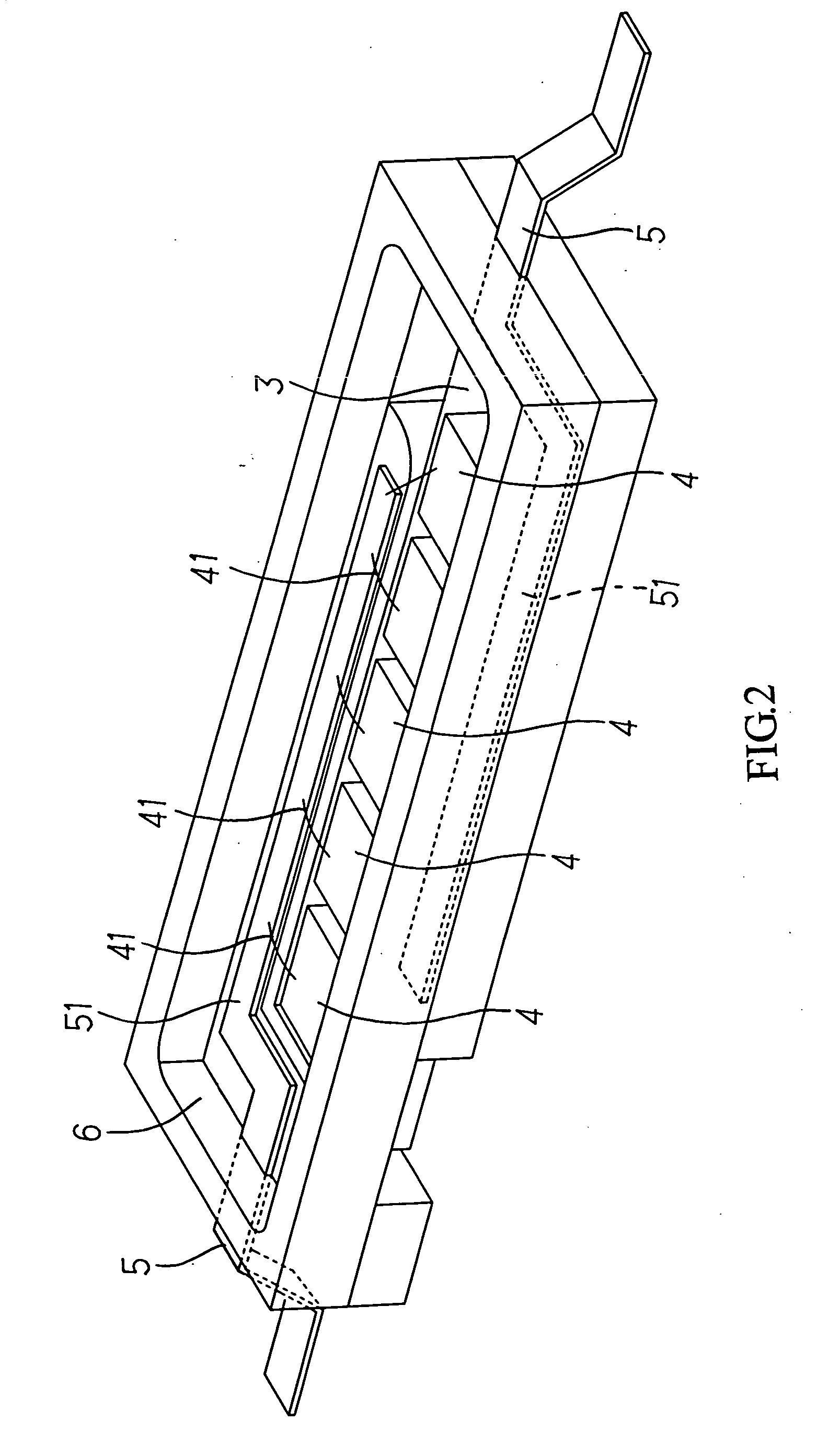
[0017] A light emitting diode package of the present invention as illustrated in FIGS. 2 and 3 includes a heat slug 3 related to an aluminum or copper substrate for the placement of multiple SMD LEDs 4 with each LED 4 selectively containing one or a plurality of light emitting chip.

[0018] Two lead frames 5 bound to both shorter sides of the heat slug 3 by means of a non-conductive material 6 with each lead frame 5 extending for a conductive area 51 respectively along both sides of the heat slug 3 in the direction of the arrangement of those LEDs 4.

[0019] The non-conductive material 6 constituting the connection between the heat slug 3 and both lead frames 5 is made in a form of a frame surrounding the sides of the heat slug 3.

[0020] When assembled, those multiple SMD LEDs 4 are placed on the heat slug 3 and plated with a gold wire 41 to respectively connect to the conductive areas 51 on both sides. The heat slug 3 is then covered up with an encapsulating material 7, and the encap...


PUM


Abstract

A package allowing agile deployment of the location of each LED chip includes a heat slug to secure multiple LED chips, two lead frames, a conducting area extending along the edge of the heat slug, and a non-conductive material that connects the heat slug and the lead frame for those multiple LED chips to connect to the conducting area by means of a gold wire without being subject to the presence of the lead frame.

Description

BACKGROUND OF THE INVENTION [0001] (a) Field of the Invention [0002] The present invention is related to a package, and more particularly to a surface mount device (SMD) package adaptable to multiple light emitting diode (LED) chips. [0003] (b) Description of the Prior Art [0004] The LED manufacturing cost has been significantly reduced thanks to continuous improvement of the LED process technologies. The LED therefore gradually exits the conventional lamps in the application areas of Xmas light, flashlight, and traffic light while taking up the LED market at a rapid expansion speed. When functioning as a backlight source for a liquid crystal display (LCD) or a lighting fixture, the LED consumes massive power, and more waste heat is generated when multiple LEDs are lighted at the same time. The waste heat from LEDs though is not at a temperature as high as that does by a tungsten filament lamp, it may prevent related circuits from providing normal functions or compromise the service...

Claims


Application Information

Patent Timeline
Patent Type & Authority Applications(United States)
IPC IPC(8): H01L33/00H01L33/50H01L33/58H01L33/62H01L33/64
CPCH01L25/0753H01L33/50H01L2224/45124H01L2224/45144H01L2224/49113H01L2224/48247H01L2224/48091H01L33/642H01L33/62H01L33/58H01L2924/00014H01L2924/00
Inventor HSIEH, HSIANG-CHENGHUANG, TENG-HUEISU, WEN-LUNG
Owner LEXTAR ELECTRONICS CORP
Why Eureka
Try Eureka