Electronic plug unit
- Summary
- Abstract
- Description
- Claims
- Application Information
AI Technical Summary
Benefits of technology
Problems solved by technology
Method used
Image

Examples
Embodiment Construction
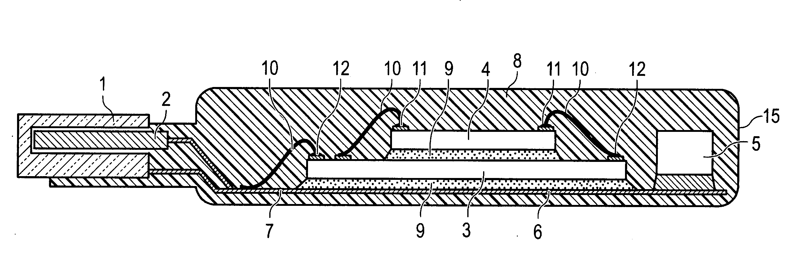
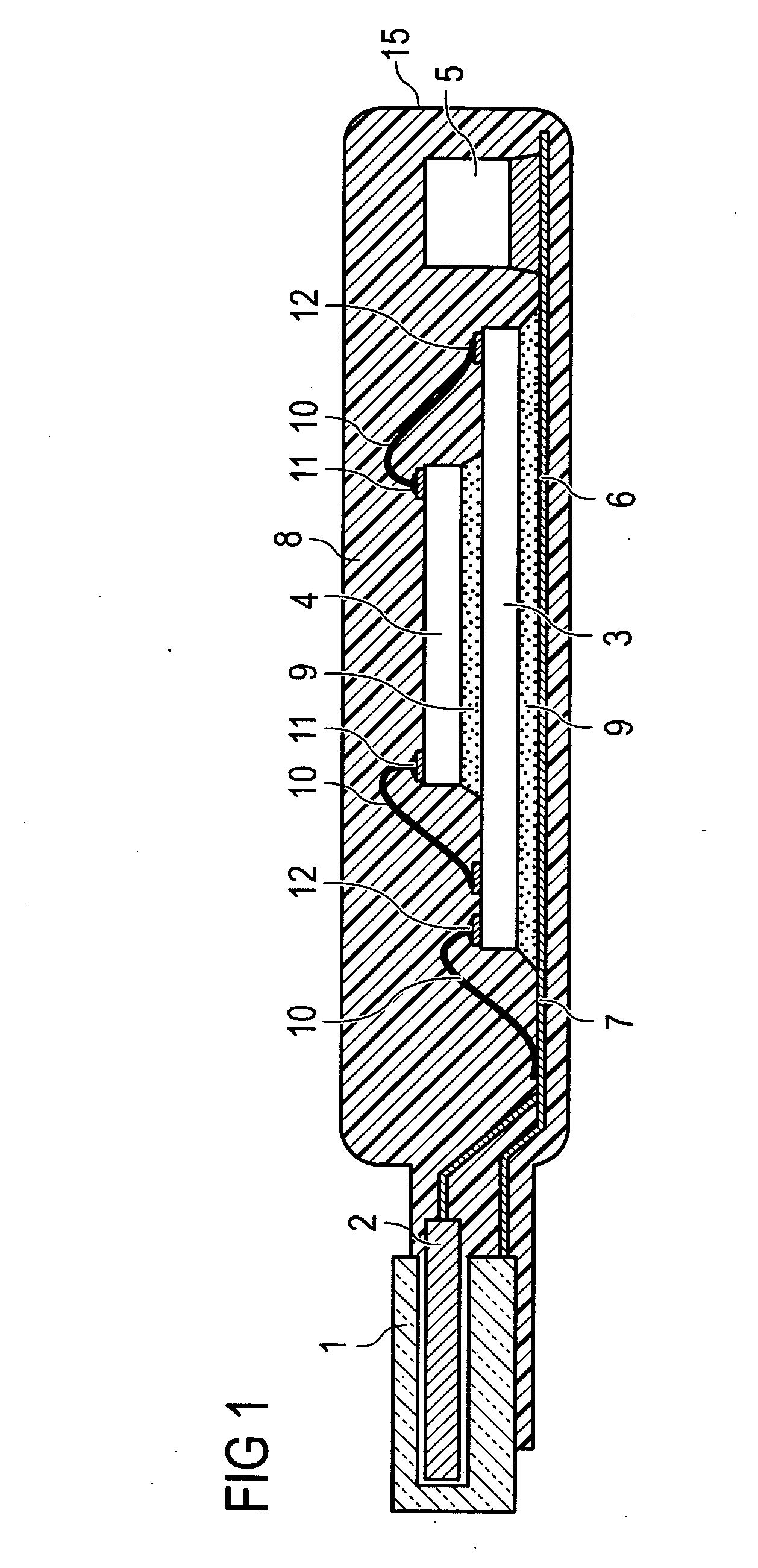
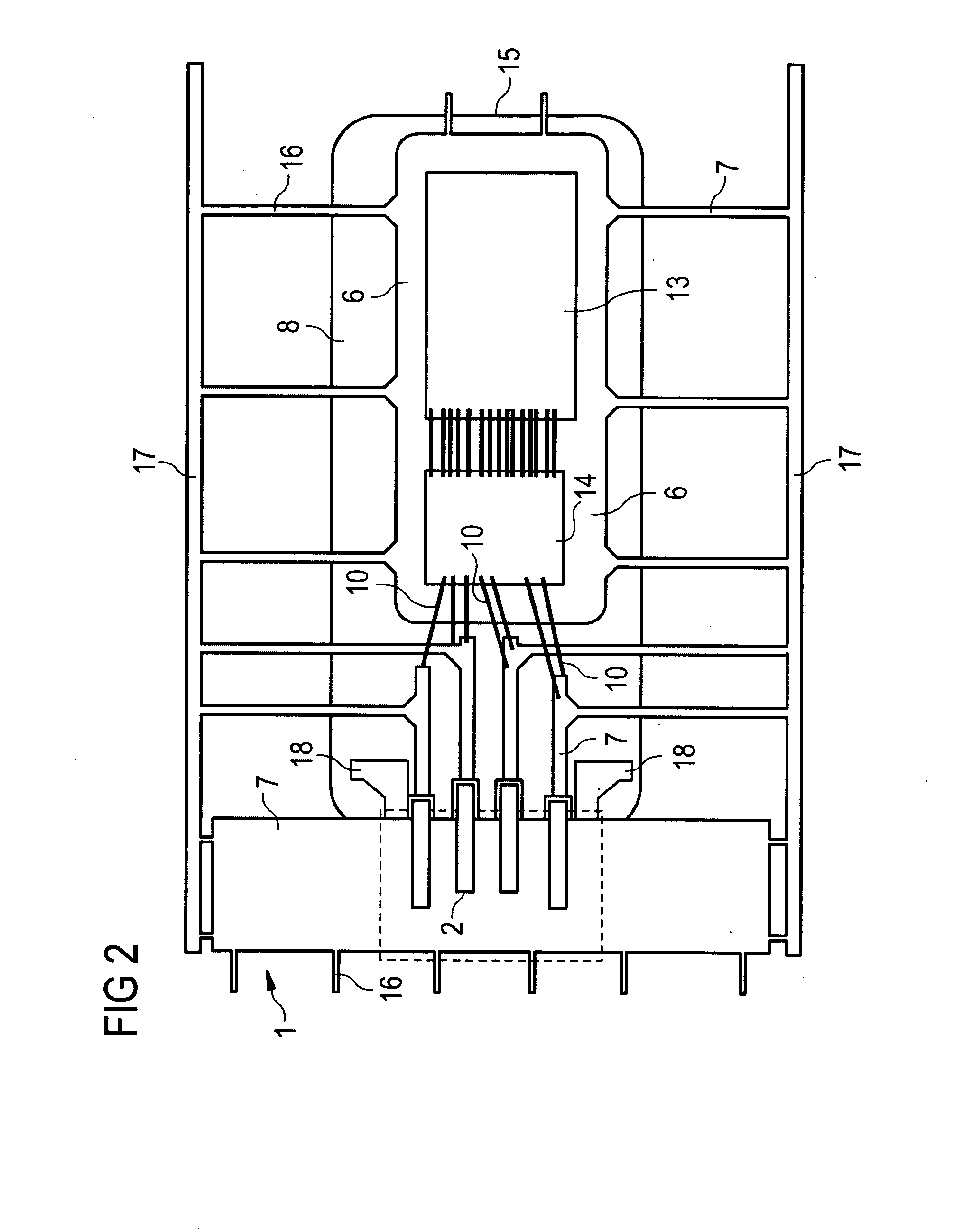
[0038]FIG. 1 is a schematic illustration of a semiconductor arrangement with a USB interface, composed of a shield 1 and contact pins 2 as well as an arrangement of stacked chips 3, 4 and an SMD (surface mount device) component 5 on a die pad 6 of a lead frame 7 with a housing 8 made of a molding material. The molding material encapsulates the lead frame 7 here with the components arranged thereon, as well as parts of the USB plug-type connector. The chips 3, 4 are mounted on the die pad 6 or on one another by means of a die attach material 9 (bonding film or the like). Wire bridges 10, for example made of gold wire, are provided for electrically connecting the chips 3, 4 to one another and to the lead frame 7.
[0039] The wire bridges 10 are drawn between bonding contacts 11 on the upper chip 4 and contacts 12 of a redistribution layer (rewiring) on the lower chip 3 and between the contacts 12 of the lower chip 3 and elements of the lead frame 7.
[0040] The molding material assumes ...
PUM
 Abstract
Description
Claims
Application Information
 - Generate Ideas
- Intellectual Property
- Life Sciences
- Materials
- Tech Scout
- Unparalleled Data Quality
- Higher Quality Content
- 60% Fewer Hallucinations
Browse by: Latest US Patents, China's latest patents, Technical Efficacy Thesaurus, Application Domain, Technology Topic, Popular Technical Reports.
© 2025 PatSnap. All rights reserved.Legal|Privacy policy|Modern Slavery Act Transparency Statement|Sitemap|About US| Contact US: help@patsnap.com