

Surface-protecting sheet and semiconductor wafer lapping method
- Summary
- Abstract
- Description
- Claims
- Application Information
AI Technical Summary
Benefits of technology
Problems solved by technology
Method used
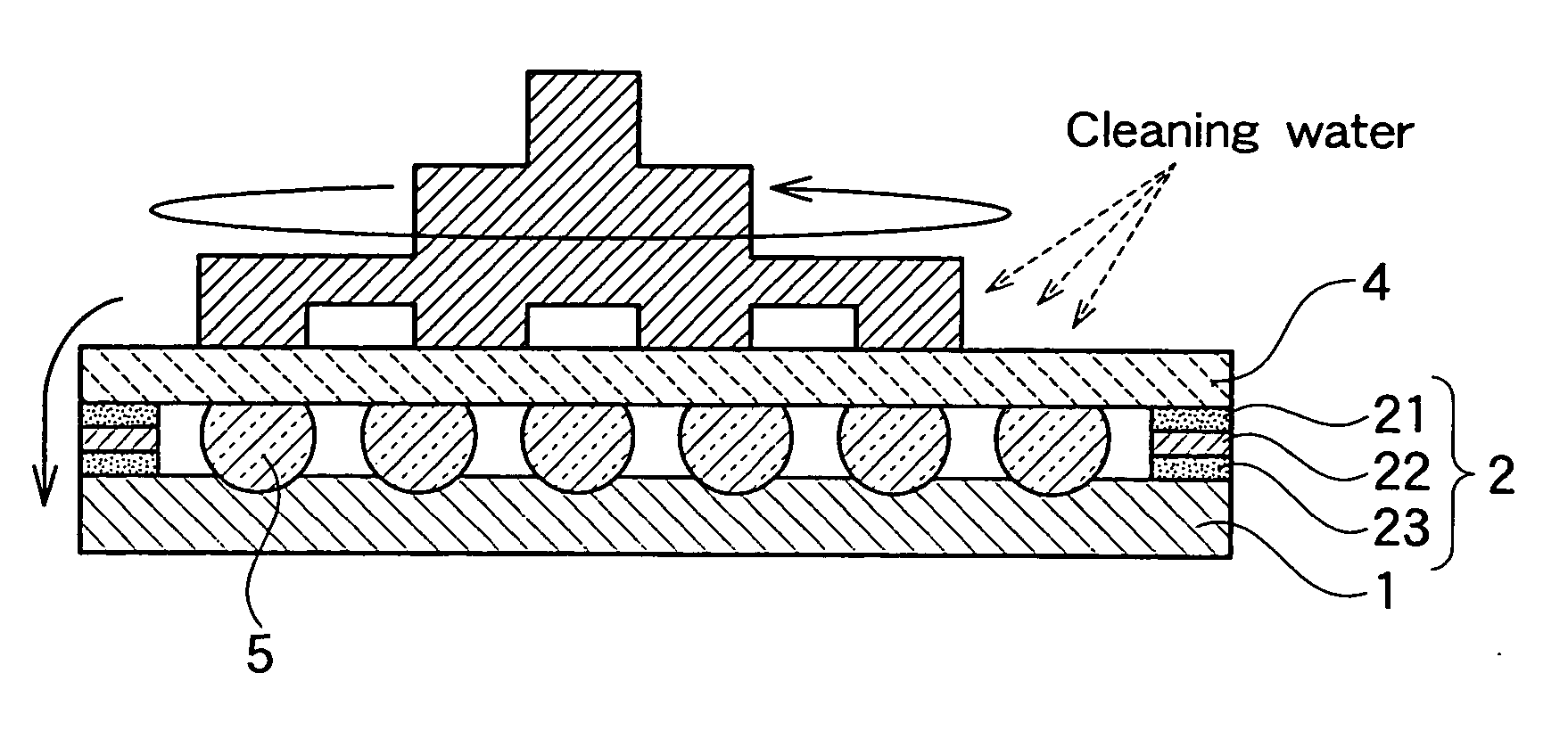
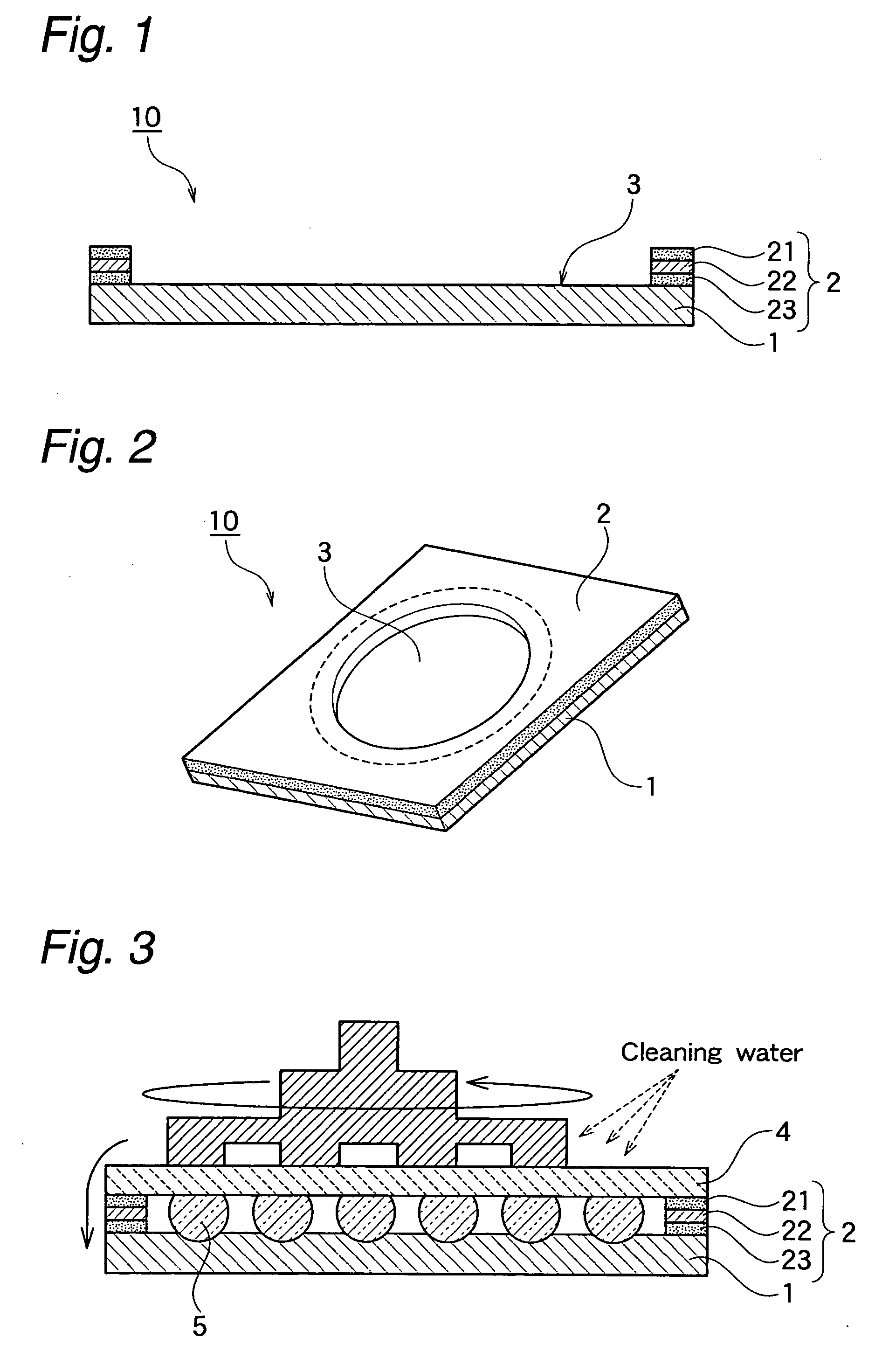
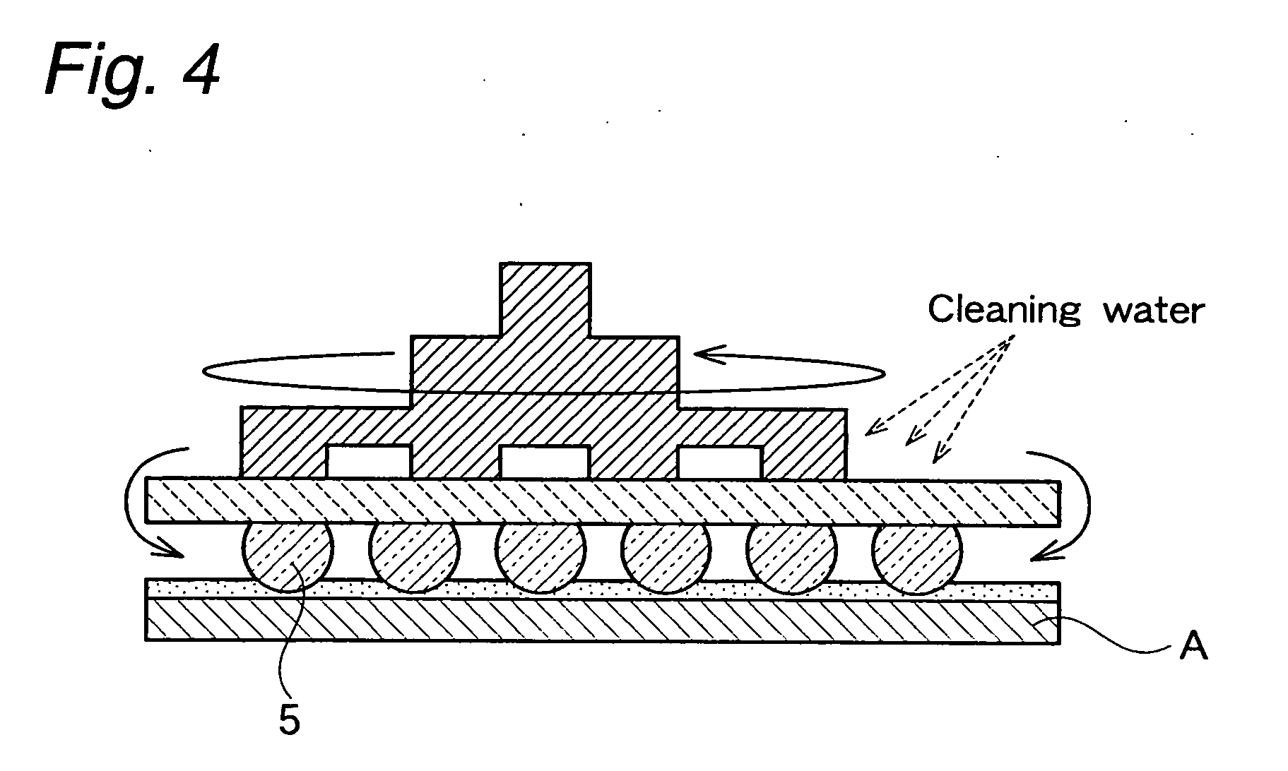
Image

Examples
example
[0052] (1) 50 Parts by weight of a urethane acrylate oligomer having a weight-average molecular weight of 5000 (available from Arakawa Chemical Industries, Ltd.), 25 parts by weight of isobornyl acrylate, 25 parts by weight of phenylhydroxypropyl acryalte, 2 parts by weight of a photopolymerization initiator (available from Ciba Specialty Chemicals Inc., Irgacure 184) and 0.2 part by weight of a phthalocyanine pigment were blended to obtain a photo-curable resin composition for cast-forming a base sheet.
[0053] The resulting resin composition was applied onto a polyethylene terephthalate (PET) film (available from Toray Industries, Inc., thickness: 38 μm) by a fountain die method in such a manner that the coating thickness became 160 μm. On the coating film, the same PET film was laminated, and then irradiation with ultraviolet rays was carried out using a high-pressure mercury lamp (160 W / cm, height: 10 cm) under the conditions of a light quantity of 250 mJ / cm2 to crosslink and cur...
PUM
| Property | Measurement | Unit |
|---|---|---|
| Height | aaaaa | aaaaa |
| Height | aaaaa | aaaaa |
| Thickness | aaaaa | aaaaa |
Abstract
Description
Claims
Application Information