Apparatus and method for memory bit-swapping-within-address-range circuit

a technology of address range and array, applied in the field of computer memories, can solve the problems of computer memory data errors, significant design complexity, and more complex controllers of drams (dynamic random-access memories)

Inactive Publication Date: 2007-03-22
CRAY
View PDF38 Cites 36 Cited by
  • Summary
  • Abstract
  • Description
  • Claims
  • Application Information

AI Technical Summary

Benefits of technology

[0014] In some embodiments, each memory controller can swap a spare bit into operation in a section of memory, dynamically in the background (i.e., in some embodiments, the swap is performed as part of the regular read-refresh operations, performed in the background during and while normal processor operations proceed in the foreground), while keeping the data in its normally addressed locations and even allowing functional processing to continue to the affected memory locations during the swap operation. One at a time, each word in the affected portion of memory is read using the normal bit mapping, corrected if necessary, and then written to the same address but using the bit-swapped mapping. Some embodiments use pointers that define the start address and end address of the bit-swapped portion of memory, such that regular processor read operations and write operations use the bit-swapped mapping for the portion that has been swapped, and use the normal bit mapping for the portion that has not been swapped. This allows the bit swapping operations and regular processor read operations and write operations to be performed at the same time (though individual operations are interleaved).

Problems solved by technology

Controllers for DRAMs (dynamic random-access memories) have been getting more complex over time as the data rates to memory have been increasing, but also as the features built into the memory parts have become more elaborate.
For example, having multiple memory banks in the memory parts (chips) adds significantly to the design complexity of a controller that attempts to use the capability of such memory parts to better advantage.
Over time and as a result of multiple causes, computer memories will have data errors.
As the density of memory chips keeps increasing, the individual memory bits become more sensitive to upset and therefore to data loss.
Data failures that do not result in (or result from) permanent IC failures, such that the memory part still functions correctly, are called soft errors.
These soft errors can be caused by familiar mechanisms like alpha particles but also, increasingly, by other mechanisms like other heavy ions and power-supply noise.
This means that soft-error rates for systems coming on line will increase by orders of magnitude over historic error-rate norms.
Other correction technologies exist, and are sometimes used, but become increasingly expensive as a fraction of total memory cost as the correction and recovery capability is improved.
A memory card design that adopts this direction has test issues, in that the memory components (the chips) are not directly accessible for testing as is normal in past industry practice, and the data rates of the high-speed interfaces are too fast for connection to testers that are available in normal production testing.
While special-purpose test equipment can be built and used, the design of special-purpose memory testers is very expensive and time consuming.

Method used


Image

  • Apparatus and method for memory bit-swapping-within-address-range circuit
  • Apparatus and method for memory bit-swapping-within-address-range circuit
  • Apparatus and method for memory bit-swapping-within-address-range circuit

Examples


Embodiment Construction

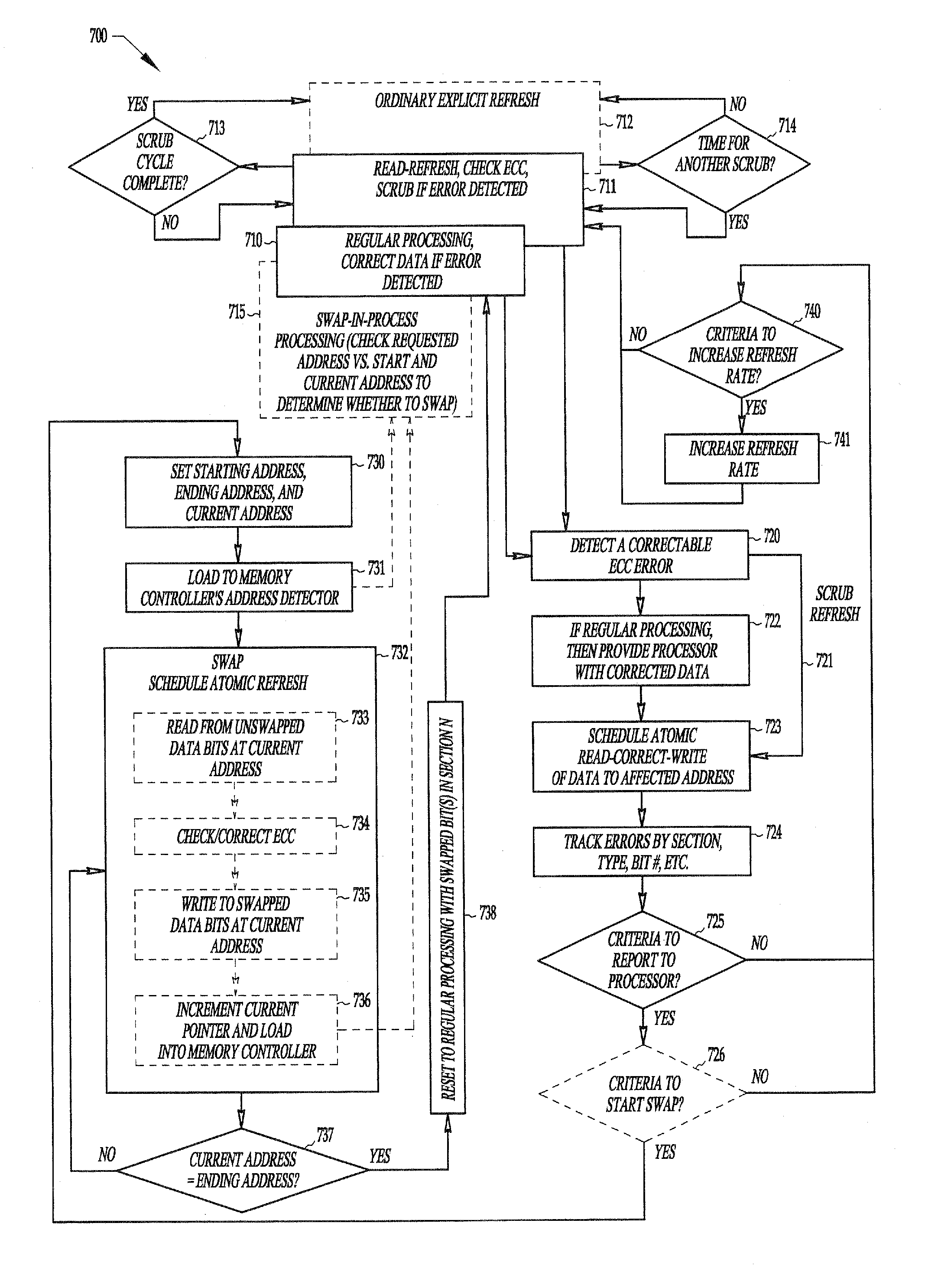
[0043] In the following detailed description of the preferred embodiments, reference is made to the accompanying drawings that form a part hereof, and in which are shown by way of illustration specific embodiments in which the invention may be practiced. It is understood that other embodiments may be utilized and structural changes may be made without departing from the scope of the present invention.

[0044] The leading digit(s) of reference numbers appearing in the Figures generally correspond to the Figure number in which that component is first introduced, such that the same reference number is used throughout to refer to an identical component which appears in multiple Figures. Signals and connections may be referred to by the same reference number or label, and the actual meaning will be clear from its use in the context of the description.

System Environment

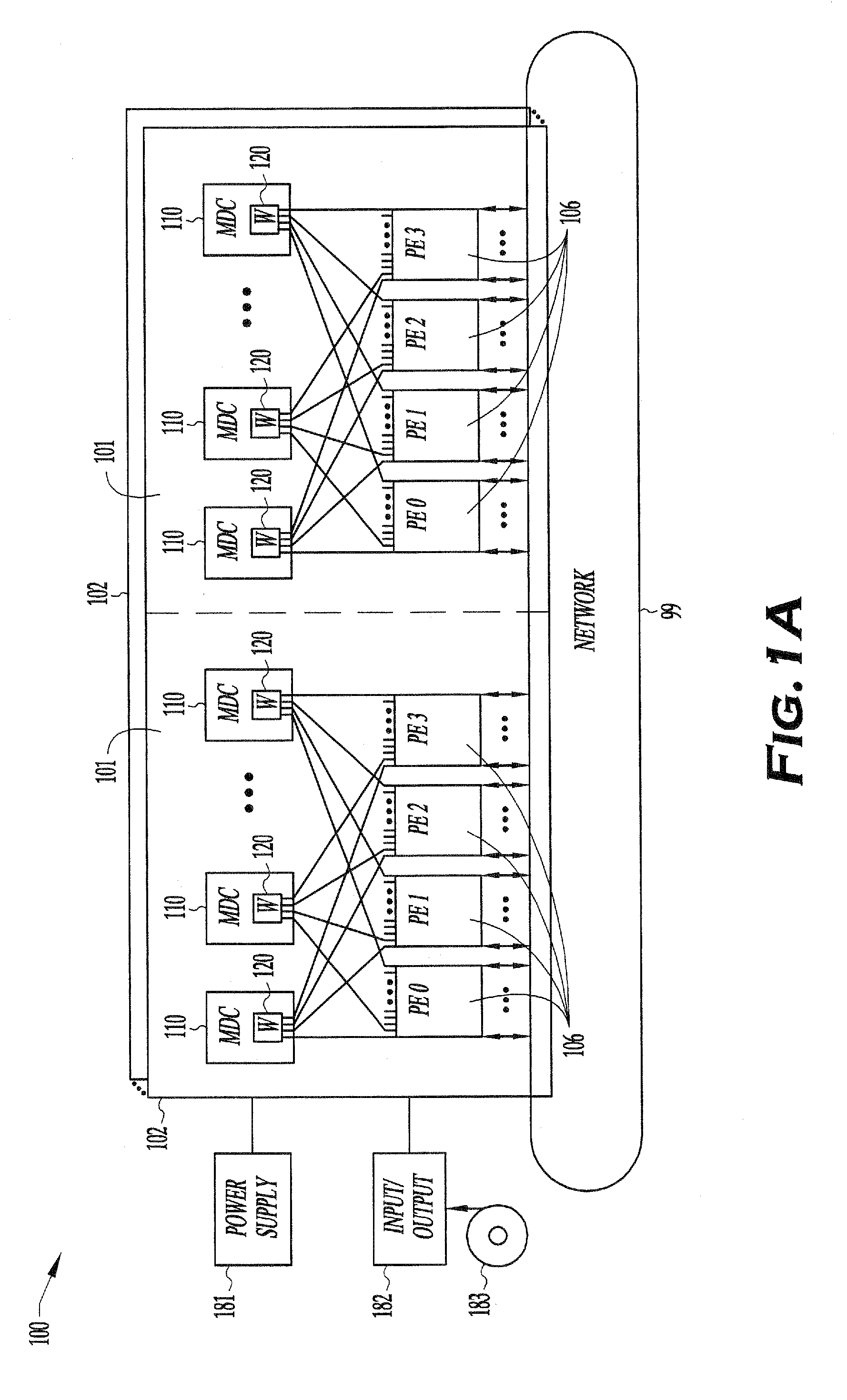
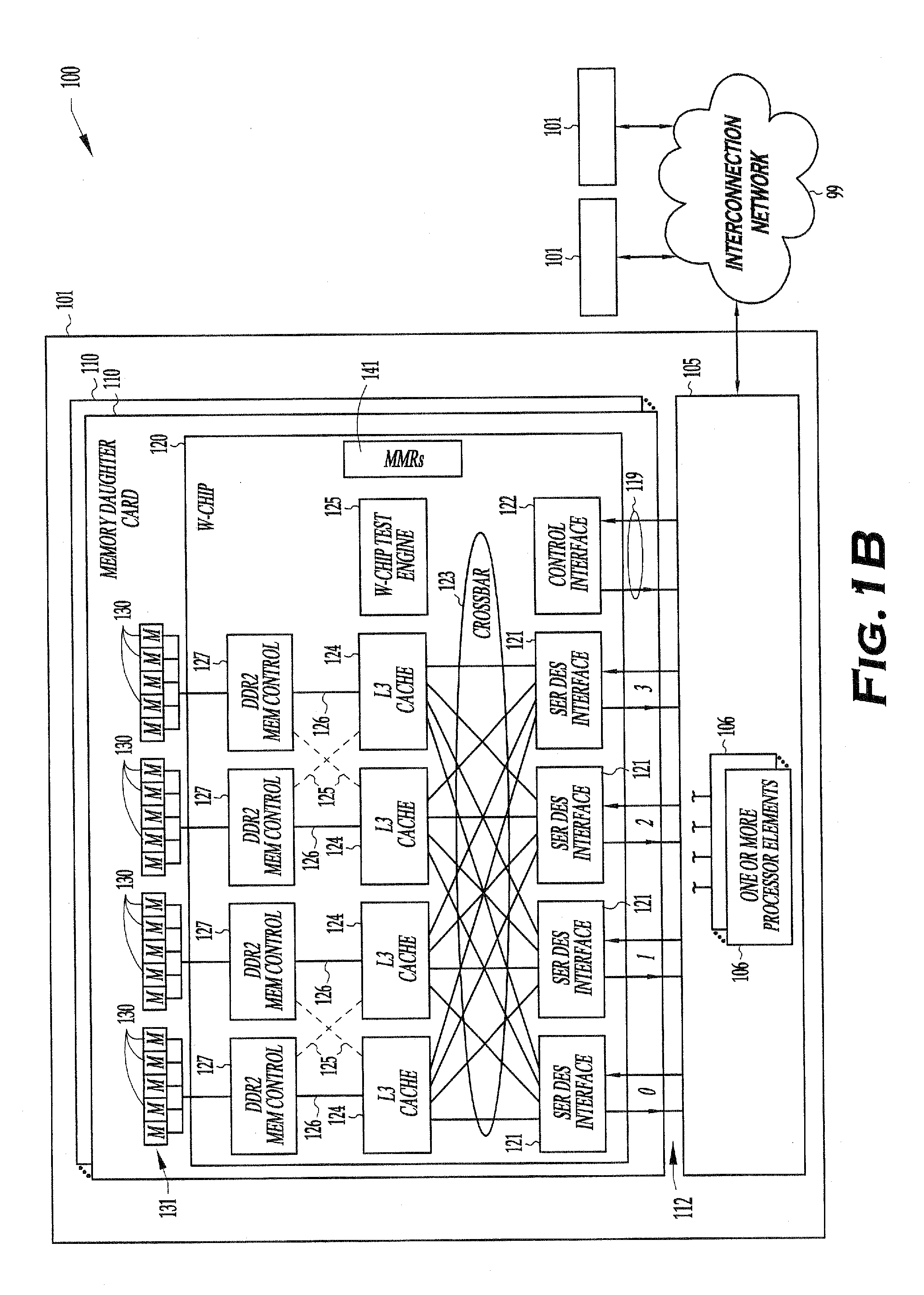
[0045]FIG. 1A is a block diagram of a computer system 100 of some embodiments of the invention. Computer system 100 inc...


PUM


Abstract

A memory controller and method that provide a read-refresh (also called “distributed-refresh”) mode of operation, in which every row of memory is read within the refresh-rate requirements of the memory parts, with data from different columns within the rows being read on subsequent read-refresh cycles until all rows for each and every column address have been read, scrubbing errors if found, thus providing a scrubbing function that is integrated into the read-refresh operation, rather than being an independent operation. For scrubbing, an atomic read-correct-write operation is scheduled. A variable-priority, variable-timing refresh interval is described. An integrated card self-tester and / or card reciprocal-tester is described. A memory bit-swapping-within-address-range circuit, and a method and apparatus for bit swapping on the fly and testing are described.

Description

RELATED APPLICATIONS [0001] This is a divisional of U.S. patent application Ser. No. 10 / 850,057 entitled “APPARATUS AND METHOD FOR MEMORY WITH BIT SWAPPING ON THE FLY AND TESTING” (Attorney Docket 1376.L02US1) filed on May 19, 2004, which claims benefit of U.S. Provisional Patent Application No. 60 / 472,174 filed on May 20, 2003, titled “APPARATUS AND METHOD FOR TESTING MEMORY CARDS,” each of which is hereby incorporated by reference in its entirety. This application is also related to U.S. patent application Ser. No. 10 / 850,044 titled “APPARATUS AND METHOD FOR TESTING MEMORY CARDS” filed May 19, 2004, U.S. patent application Ser. No. 11 / 558,450 titled “APPARATUS AND METHOD FOR MEMORY READ-REFRESH, SCRUBBING AND VARIABLE-RATE REFRESH” (Attorney Docket 1376.L01US1) filed on even date herewith, and [0002] U.S. patent application Ser. No. 11 / 558,452 titled “APPARATUS AND METHOD FOR MEMORY ASYNCHRONOUS ATOMIC READ-CORRECT-WRITE OPERATION” (Attorney Docket 1376.L03US1) filed on even d...

Claims


Application Information

Patent Timeline
Patent Type & Authority Applications(United States)
IPC IPC(8): G06F13/28G06F11/10G06F11/20G11C29/00G11C29/44
CPCG06F11/106G11C11/401G11C2029/0401G11C29/4401G11C29/848G11C29/44
Inventor DIXON, R. PAULRESNICK, DAVID R.SNYDER, VAN L.
Owner CRAY
Why Eureka
Try Eureka