Data storing method of dynamic RAM and semiconductor memory device

a dynamic ram and data storing technology, applied in the field of data storing methods of dynamic rams (random access memory) and semiconductor memory devices, can solve the problems of increasing current consumption, reducing the amount of current in the refreshing operation,

Inactive Publication Date: 2006-05-23
LONGITUDE SEMICON S A R L
View PDF17 Cites 55 Cited by
  • Summary
  • Abstract
  • Description
  • Claims
  • Application Information

AI Technical Summary

Benefits of technology

[0013]The outline of another one of representative inventions disclosed in the application will be described as follows. A semiconductor integrated circuit device has: a memory circuit including a dynamic memory cell and having an information retaining mode during which data is not read/written from/to other circuits; and a data retention control circuit including an ECC circuit and a refresh cycle setting circuit. When the dynamic RAM enters an operation mode of performing only an

Problems solved by technology

In other words, the CPU or ECC circuit has to operate in order to extend the refresh cycle, and it causes a problem such that a reduced amount o

Method used


Image

  • Data storing method of dynamic RAM and semiconductor memory device
  • Data storing method of dynamic RAM and semiconductor memory device
  • Data storing method of dynamic RAM and semiconductor memory device

Examples


Embodiment Construction

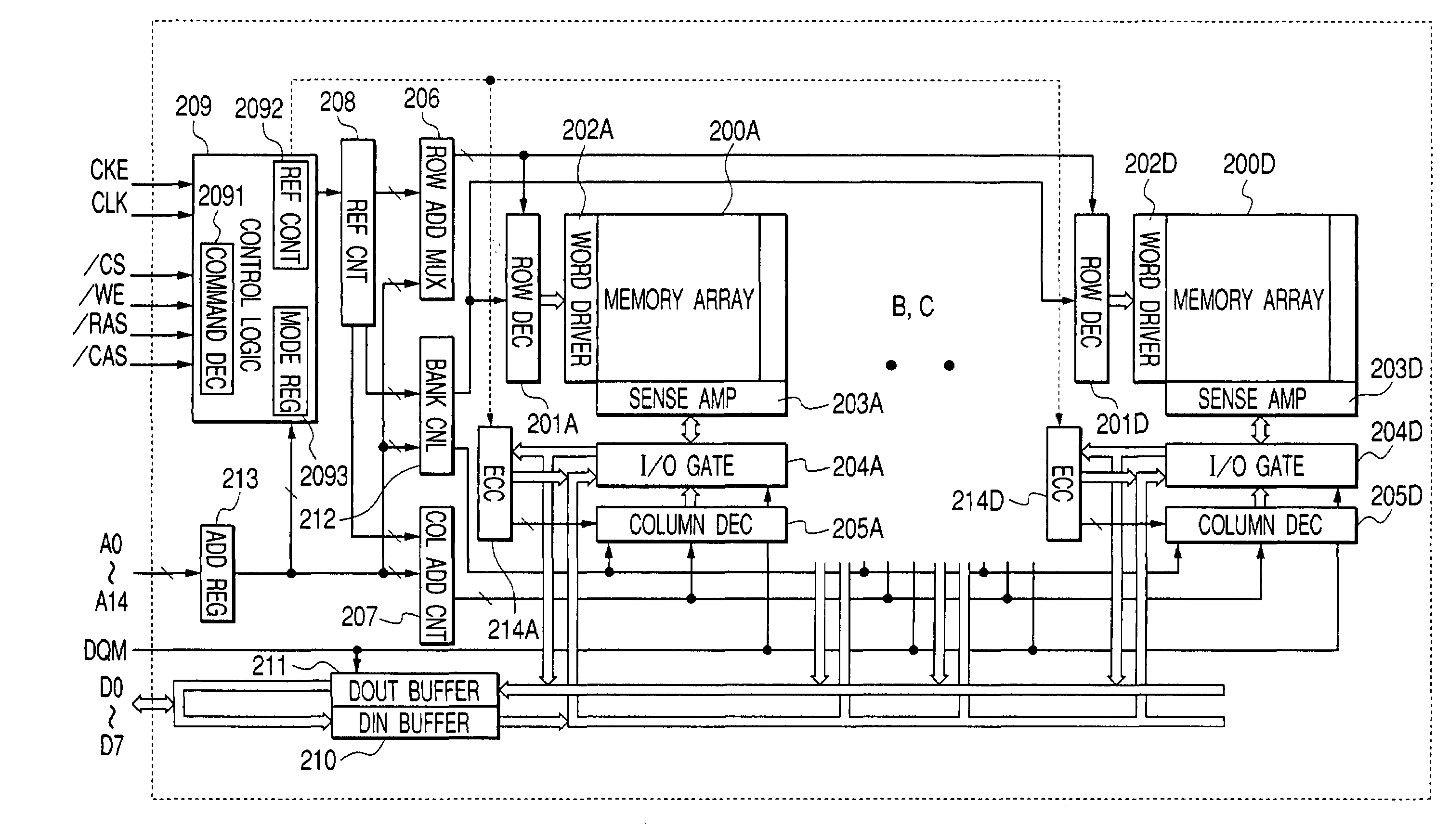
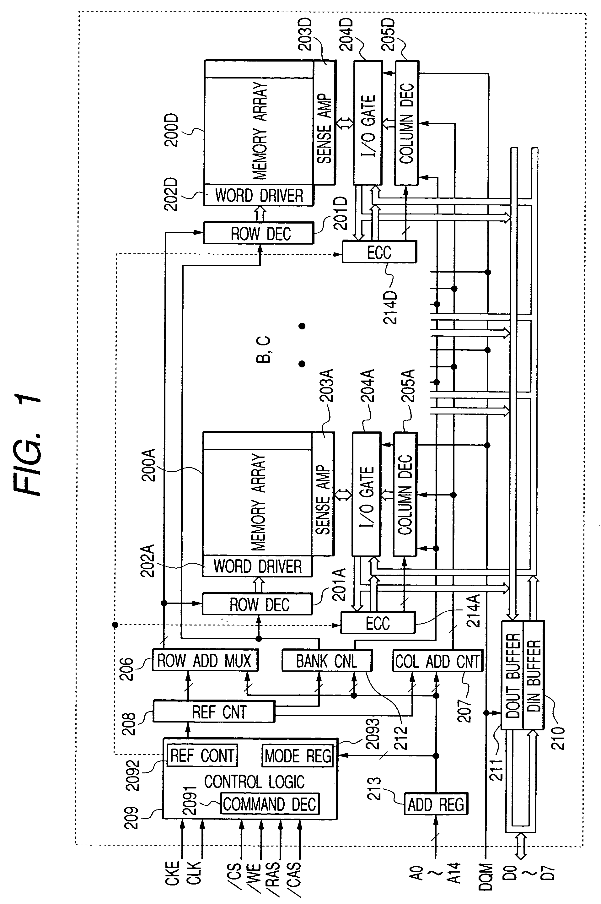
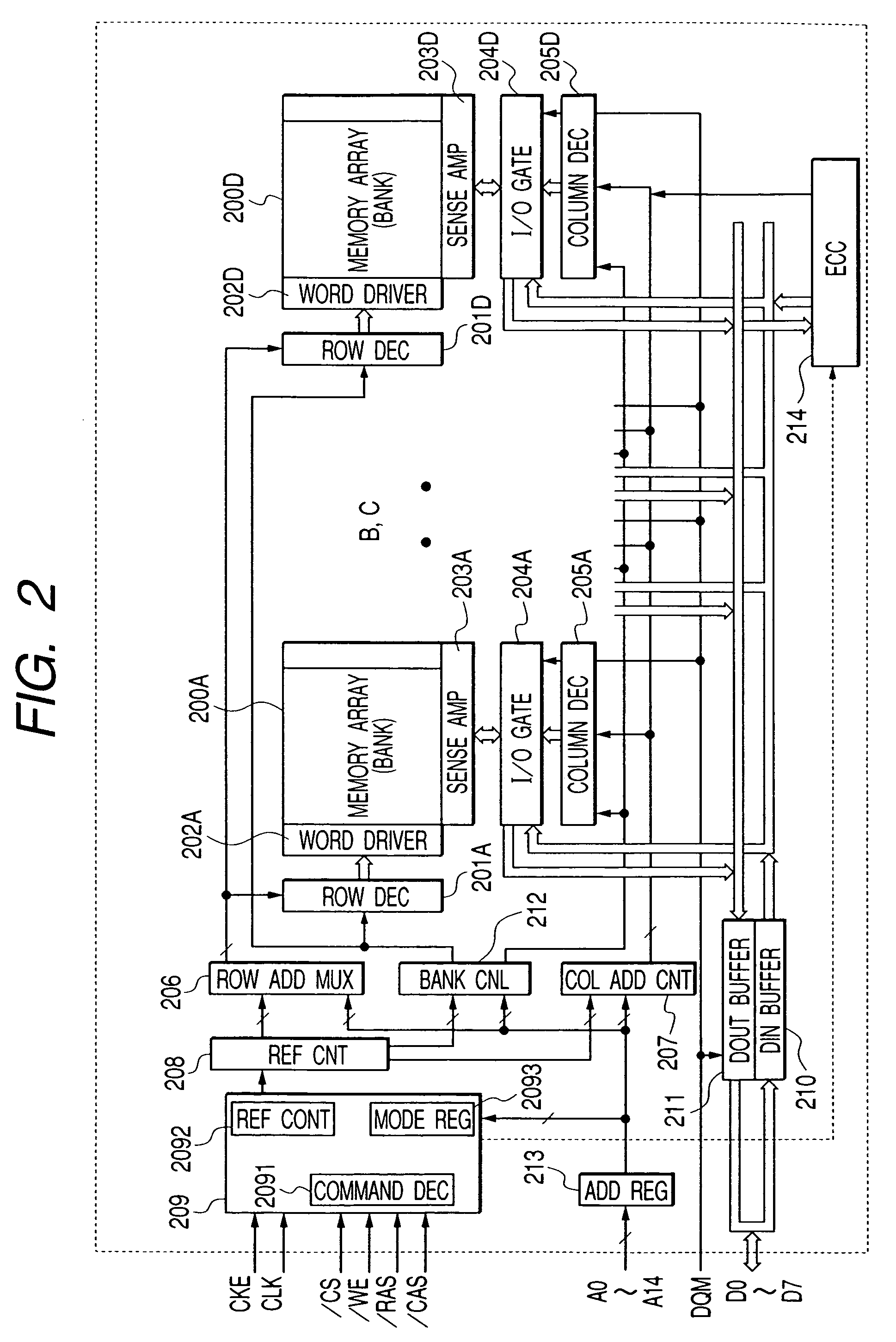
[0050]FIG. 1 is a general block diagram showing an example of a dynamic RAM (hereinbelow, simply called DRAM) according to the invention. The DRAM of the example is directed to an SDRAM (Synchronous Dynamic Random Access Memory). The SDRAM of the example has, but not limited, four memory arrays 200A to 200D in correspondence with four memory banks. The diagram illustrates two memory arrays 200A and 200D out of the four memory arrays 200A to 200D. Each of the memory arrays 200A to 200D corresponding to the four memory banks 0 to 3 has dynamic memory cells arranged in a matrix. A terminal for selecting memory cells arranged in the vertical direction of the memory array in the diagram is coupled to a word line (not shown), and data input / output terminals of memory cells arranged in the lateral direction are coupled to complementary data lines (not shown) every row.

[0051]One of the not-shown word lines of the memory array 200A is driven to a selection level in accordance with a decoding...


PUM


Abstract

When a DRAM enters an operation mode in which only a data storing operation is performed, a check bit for error detection and correction for plural data is generated and stored. Refresh operation is performed in a refresh cycle which is made long within an allowable range of an error occurrence by an error correcting operation using the check bit. Before the DRAM returns to the normal operation mode from the data holding operation mode, an error bit is corrected by using the data and the check bit.

Description

CROSS-REFERENCE TO RELATED APPLICATION[0001]This application is a continuation of Application Ser. No. 09 / 923,405 filed Aug. 8, 2001 now U.S. Pat. No. 6,697,992.BACKGROUND[0002]The present invention relates to a data storing method of a dynamic RAM (Random Access Memory) and a semiconductor memory device and, more particularly, to a technique effective for use in a data storing technique in a memory circuit having dynamic memory cells.[0003]It was found by the search made after the present invention was achieved that Japanese Unexamined Patent Publication Nos. Hei11(1999)-213659 (corresponding to U.S. Pat. No. 6,199,139, hereinbelow, called prior art 1) and Hei 7(1995)-262794 (hereinbelow, called prior art 2) seem to be related to the present invention to be described hereinlater. According to prior art 1, to optimize the refresh cycle interval of a DRAM in a sleep mode, the frequency of the refresh cycle is controlled by software under the control of a CPU by using the number of er...

Claims


Application Information

Patent Timeline
IPC IPC(8): H03M13/00G11C29/00G11C11/4078G06F11/10G11C7/10G11C11/401G11C11/406G11C11/4093G11C29/42
CPCG06F11/1008G06F11/106G11C7/1006G11C7/1045G11C11/4093G11C11/4096G11C11/406G06F11/108G11C2207/104G11C2211/4062G11C11/4078
Inventor ITO, YUTAKAIWAI, HIDETOSHI
Owner LONGITUDE SEMICON S A R L
Why Eureka
Try Eureka