Systems and methods for additive deposition of materials onto a substrate

a technology of additive deposition and substrate, which is applied in the field of printing systems, can solve the problems of inability to meet the stringent design requirements of printed electronics, the current knowledge of the technology of fully additive printing electronics, and the slow and well known process

Inactive Publication Date: 2007-03-29
WEYERHAEUSER CO
View PDF36 Cites 53 Cited by
  • Summary
  • Abstract
  • Description
  • Claims
  • Application Information

AI Technical Summary

Problems solved by technology

This well known process is slow, complex, expensive and impractical for producing low-cost electronic devices.
However, no suitable fully additive process for printing electronics is currently known in the art.
While conventional printing techniques are capable of reproducing both vector and raster images, they cannot easily meet many of the stringent design requirements of printed electronics, including, for example, (a) the ability to deposit very precise amounts of material onto a substrate; (b) the ability to render very thin lines and spacings on the order of, for example, approximately three (3) microns; (c) the ability to transfer extremely uniform and ultra thin layers of material on the order of, for example, approximately 50-100 nanometers; (d) the ability to achieve print registration within, for example, approximately 25 microns from layer to layer; and (e) the ability to render sharp and continuous edges.
While flexographic, gravure, and lithographic printing presses of the type shown in FIGS. 10-12, as well as other analog printing presses, such as letterpress, etc., work well in traditional printing applications, such as newspaper printing, magazine printing, package printing, etc., these analog techniques suffer many drawbacks that would potentially affect both the capability of printing electronic devices and the reliability of the resulting printed electronic devices.
One such drawback is the inability of some analog presses to print crisp and continuous lines and solids, which are used extensively in printed electronics.
However, while screening works well for photographs, screening results in spaced dots with poor ink spread, as well as missing dots (caused by rough surfaces preventing good contact between the plate and the substrate).
Spaced dots with poor ink spread and missing dots compromise continuity of the rendered layer, which may result in non-functional electronic devices.
Another drawback of analog or contact type printing presses is the inability of analog printing presses to reliably meter and uniformly transfer very thin (e.g., 5-100 nanometers) layers of ink onto a substrate due to, among others, the conventional anilox or metering roll.
For example, in flexographic presses, the inherent attributes of the anilox roll (i.e., cell frequency) and the physical means of transferring ink to the print cylinder results in inaccurate and non-constant ink film thicknesses once the ink is transferred from the printing plate to the substrate.
Additionally, the use of doctor blades in both flexography and gravure may cause uneven ink distribution along the print cylinders, resulting in non-uniform layers when deposited on the substrate.
Yet another drawback of analog or contact type printing presses is the inability to render very small features, such as traces, electrodes, etc.
Reliably printing three micron features is not currently attainable by conventional printing presses.
Finally, many conventional analog presses are not able to meet the registration tolerance of approximately 25 microns called for in many printed electronic design specifications.
For example, a typical commercial lithography press can achieve a registration error on the order of a row's spacing of half-tone dots.
Even with tighter control, registration could be achieved only “on average,” which means that actual registration from print to print could vary substantially thereby considerably reducing device yield.
Problems with printing electronic devices are not only limited to contact-type printing presses.
However, digital printing techniques are not without their problems.
However, like gravure printing presses, inkjet printing is inherently a screening process, and thus, does not render vector images as well as raster images.
Specifically, inkjet printing results in jagged edges, and inconsistent and non-continuous solids.
Additionally, inkjets also tend to produce a wavy film consisting of a layer of individual ink drops, and may result in non-uniform layer thicknesses.
Such problems can potentially affect printing electronic operations and reliability.

Method used


Image

  • Systems and methods for additive deposition of materials onto a substrate
  • Systems and methods for additive deposition of materials onto a substrate
  • Systems and methods for additive deposition of materials onto a substrate

Examples


Embodiment Construction

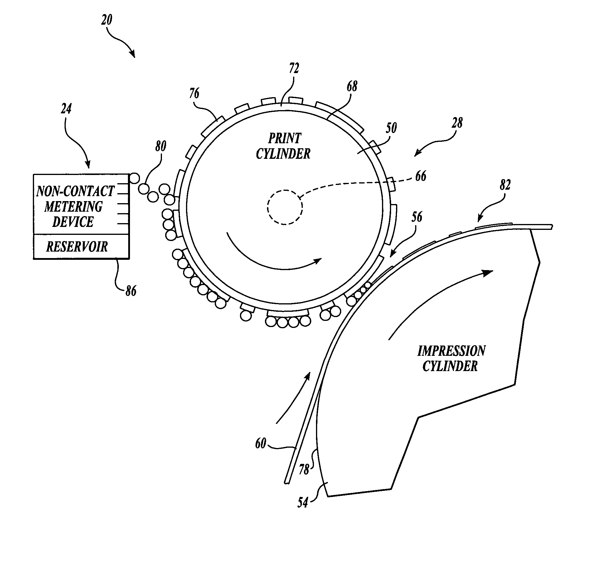
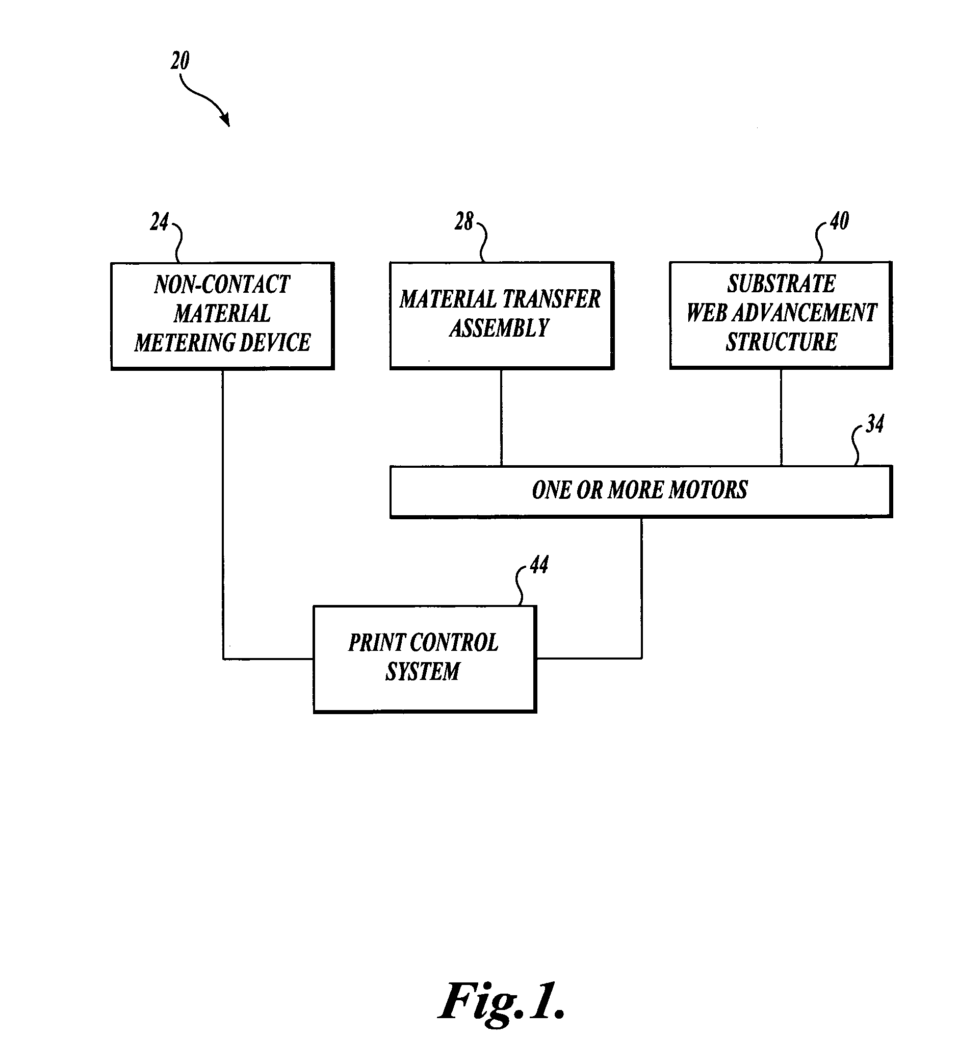
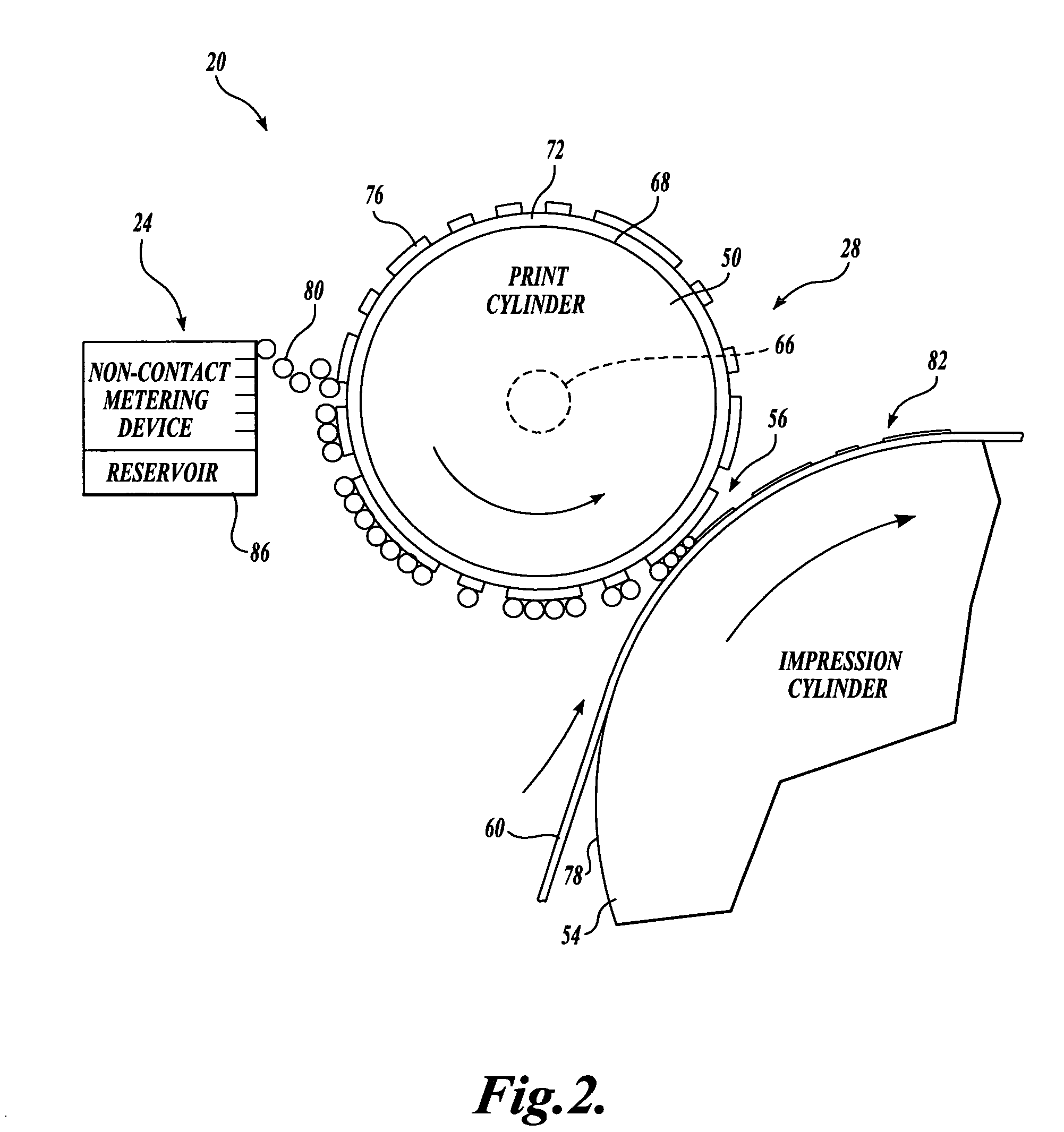
[0036] Embodiments of the present invention will now be described with reference to the accompanying drawings where like numerals correspond to like elements. The following description provides examples of systems and methods for fabricating printed electronic devices with polymeric and non-polymeric materials in a fully additive process. The systems and methods of the present invention may also be suitable for use in printing color graphics, or to color, coat, varnish, or apply other surface treatments to a variety of substrates. The following examples generally describe the systems and methods as a two stage printing process that includes a digital first stage in the form of a non-contact material metering device, such as one or more digital inkjet heads, vapor deposition systems, aerosol systems, etc., for selectively discharging a metered quantity of material, and an analog second stage, such as flexographic print and impression cylinders, for transferring the material deposited...


PUM


Abstract

A two stage printing process that includes a digital first stage in the form of a non-contact material metering device, such as one or more digital inkjet heads, for selectively discharging a metered quantity of material, and an analog second stage, such as flexographic print and impression cylinders, for transferring the material deposited thereon by the non-contact material metering device onto a substrate.

Description

FIELD OF THE INVENTION [0001] Embodiments of the present invention relate generally to printing systems, and more particularly, to printing systems and methods for depositing one or more layers of material in an additive process. BACKGROUND OF THE INVENTION [0002] Electrically conducting and semiconducting organic polymers have become available in recent years. Along with conventional insulating polymers, conducting and semiconducting organic polymers enable the construction of micro-electronic components or complete circuits on flexible substrates using polymers. Some examples of micro-electric components that may be produced include capacitors, resistors, diodes, and transistors, while examples of complete circuits may include RFID tags, sensors, flexible displays, etc. [0003] Currently, these polymer electronic components and circuits are fabricated by well known subtractive processes in which polymer deposition onto the substrate is followed by removal, i.e., by etching, of unwa...

Claims


Application Information

Patent Timeline
Patent Type & Authority Applications(United States)
IPC IPC(8): B41F5/00B41F7/00B41J2/01
CPCB41J2/0057H01L51/56H01L51/0004H10K71/13H10K71/00
Inventor HIRAHARA, EDWINLEE, DAVID L.
Owner WEYERHAEUSER CO
Why Eureka
Try Eureka