Light emitting device

Inactive Publication Date: 2007-03-29
IND TECH RES INST
View PDF3 Cites 10 Cited by
  • Summary
  • Abstract
  • Description
  • Claims
  • Application Information

AI Technical Summary

Benefits of technology

[0017] Compared with the prior art, the light emitting device of the present invention achieves a much simpler light emitting device of thin thickness by combining a light emitting element with a base member which is connected to the

Problems solved by technology

In addition, since the LED chip is electrically connected to the outside through the aluminum or ceramic substrate, the conductive path is very long, which results in too much heat absorption by the aluminum or ceramic substrate, thereby making the mass production difficult.
Furthermore, if several chip products are applied to the aluminum or ceramic substrate, the aluminum or ceramic substrate becomes so weak that it needs to be processed before the reflow process, thereby resulting in high fabrication cost.
In the above two packa

Method used


Image

  • Light emitting device
  • Light emitting device
  • Light emitting device

Examples


Embodiment Construction

[0030] Hereunder, embodiments of the present invention will be described in full detail with reference to the accompanying drawings.

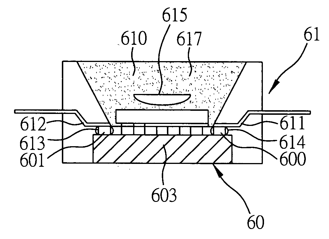
[0031] FIGS. 7(A) to 7(E) are diagrams showing detailed structure of a light emitting device according to the present invention. The light emitting device of the present invention at least includes a light emitting element 60 (shown in FIG. 7(A)) and a base member 61 (shown in FIG. 7(B)) to which the light emitting element 60 can be mounted.

[0032] As shown in FIG. 7(A), the light emitting element 60 has at least two electrodes 600 and 601 disposed at the side of the light output surface of the light emitting element 60 for power connection. Preferably, the light emitting element 60 includes at least one light emitting chip 602 and at least one substrate 603 provided with electrodes 600 and 601 for power connection. The light emitting chip 602 in a flip chip configuration is mounted to the substrate 603 and electrically connected with the substrate 603...


PUM


Abstract

A light emitting device is proposed, which emits light while connected to the power. The light emitting device includes a light emitting element having at least two electrodes disposed at the side of the light output surface thereof; and a base member having a recess and lead portions corresponding to the electrodes, the light emitting element being mounted on the base member and received in the recess, wherein the light output surface faces toward opening of the recess that becomes smaller while approaching the light output surface, and the electrodes are respectively in electrical connection with the lead portions that extend from the connection positions to outer edge of the base member for power connection. The light emitting device of the present invention has advantages of short current path, low series thermal resistance and low cost. In addition, the depth of the recess can further be increased to improve light collecting efficiency.

Description

BACKGROUND OF THE INVENTION [0001] 1. Field of the Invention [0002] The present invention relates to light emitting devices and, more particularly, to a light emitting device that can be applied to high power light emitting diodes. [0003] 2. Description of Related Art [0004] Currently, light emitting diodes (LEDs) that are characterized by long lifetime, small volume, low heat dissipation, low power consumption, fast response speed and single color light emission are widely used in indicator lights, bill boards, traffic lights, auto lamps, display panels, communication tools, consumer electronics and so on. Accordingly, different packaging techniques are developed for LEDs packaging, which results in different package structures of LEDs. [0005] FIGS. 1(A) to 1(C) show a flip chip packaging process. As shown in FIG. 1(A), a plurality of conductive bumps 11 is formed on an aluminum substrate 10. Then, as shown in FIG. 1(B), an LED chip 12 is attached to the aluminum substrate 10 upsid...

Claims


Application Information

Patent Timeline
IPC IPC(8): H01L33/00H01L33/58H01L33/50H01L33/60H01L33/62
CPCH01L33/60H01L33/62H01L33/642H01L2224/16H01L2924/01079H01L2224/48091H01L2924/00014H01L2924/01068
Inventor LIN, MING-TELIN, MING-YAOKUO, CHIA-CHANGHUANG, SHENG-PANYEH, WEN-YUNG
Owner IND TECH RES INST
Why Eureka
Try Eureka