Silicon carbide MOS device

A technology of MOS devices and silicon carbide, which is applied in the direction of semiconductor devices, electrical components, circuits, etc., can solve the problems of increasing current flow path, poor device stability, reliability problems, etc., to increase the number of devices, low on-resistance, The effect of reducing production costs

Pending Publication Date: 2021-02-23
江西万年芯微电子有限公司
View PDF3 Cites 0 Cited by
  • Summary
  • Abstract
  • Description
  • Claims
  • Application Information

AI Technical Summary

Problems solved by technology

Although silicon carbide UMOSFET has lower on-state resistance and more compact cell layout, due to the problem of excessive electric field of the bottom gate oxide layer, it brings reliability problems to the long-term use of silicon carbide UMOSFET, resulting in poor long-term stability of the device
[0003] In the prior art, in the process of setting the gate oxide layer, the horizontal setting method is often adopted, which will increase the current flow path, thus making the on-resistance larger

Method used


Image

  • Silicon carbide MOS device

Examples


Embodiment Construction

[0017] The implementation of the present invention will be described in detail below with reference to the drawings and examples, so as to fully understand and implement the implementation process of how to use technical means to solve technical problems and achieve technical effects in the present invention.

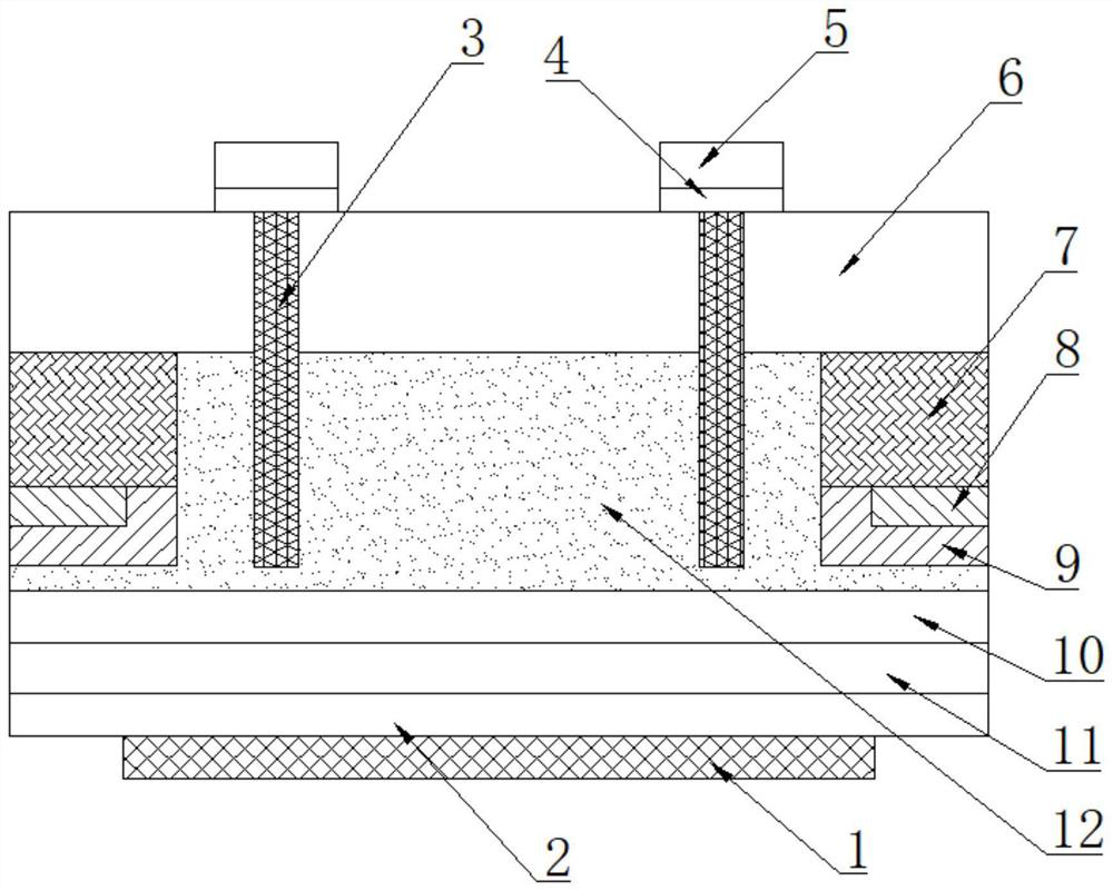
[0018] Specific embodiments of the present invention such as figure 1 As shown, a silicon carbide MOS device includes a metal drain, the upper end surface of the metal drain is provided with a drain electrode, the upper end surface of the drain electrode is provided with an N+ type silicon carbide substrate, and the N+ type silicon carbide The upper end surface of the substrate is provided with an N-type silicon carbide drift region, and a silicon carbide N- epitaxial layer is grown on the upper end surface of the N-type silicon carbide drift region; the upper left and upper right of the silicon carbide N- epitaxial layer have sources There is a silicon carbide P+ doped...


PUM

PropertyMeasurementUnit
depthaaaaaaaaaa
depthaaaaaaaaaa
electrical resistivityaaaaaaaaaa

Abstract

The invention discloses a silicon carbide MOS device which comprises a metal drain electrode. A drain electrode is arranged on the upper end face of the metal drain electrode, an N+ type silicon carbide substrate is arranged on the upper end face of the drain electrode, and an N type silicon carbide drift region is arranged on the upper end face of the N+ type silicon carbide substrate. A siliconcarbide N-epitaxial layer grows on the upper end face of the N type silicon carbide drift region, source trenches are formed at the left upper side and the right upper side of the silicon carbide N-epitaxial layer, and a silicon carbide P+ doped region and a silicon carbide P-type doped region are arranged below the source trenches from top to bottom. Source metal is arranged on the upper end faceof the silicon carbide N-epitaxial layer, and through grooves are formed in the silicon carbide N-epitaxial layer and the source metal. Gate oxide layers are arranged on the inner walls and the outersurfaces of the grooves, gate low-resistance deposits are arranged in the grooves, and a gate oxide layer, a gate low-resistance deposit and gate metal are sequentially arranged at the top ends of the grooves from bottom to top. According to the invention, the gate oxide layer is arranged to be longitudinal and is embedded into the silicon carbide body, and the current path is shorter during conduction, so that the conduction resistance is lower, and the current capability is stronger.

Description

technical field [0001] The invention relates to the technical field of semiconductors, in particular to a silicon carbide MOS device. Background technique [0002] Silicon carbide MOSFET devices are next-generation semiconductor devices made of silicon carbide, a wide bandgap semiconductor material. Many attractive characteristics of silicon carbide materials, such as 10 times the critical breakdown electric field strength of silicon materials, high thermal conductivity, large band gap and high electron saturation drift velocity, etc., make SiC materials become the international power semiconductor The research hotspots of devices, and in high-power applications, such as high-speed railways, hybrid vehicles, intelligent high-voltage direct current transmission, etc., silicon carbide devices have been given high expectations. At the same time, silicon carbide power devices have a significant effect on reducing power loss, making silicon carbide power devices known as "green ...

Claims


Application Information

Patent Timeline
Patent Type & Authority Applications(China)
IPC IPC(8): H01L29/78H01L29/423H01L29/06
CPCH01L29/7813H01L29/4236H01L29/0619
Inventor 艾育林
Owner 江西万年芯微电子有限公司
Why Eureka
Try Eureka