Depletion mode field effect transistor device and preparation method thereof

A field-effect transistor, depletion-mode technology, used in semiconductor/solid-state device manufacturing, semiconductor devices, electrical components, etc., can solve the problems of low withstand voltage, large leakage current, and large on-resistance of the device, and achieve a short current path. , The effect of low on-resistance and high breakdown voltage

Pending Publication Date: 2021-07-20
SHANGHAI CHANGYUAN WAYON MICROELECTRONICS
View PDF0 Cites 0 Cited by
  • Summary
  • Abstract
  • Description
  • Claims
  • Application Information

AI Technical Summary

Problems solved by technology

[0004] However, the existing depletion-type MOS has a large on-resistance in the on state; in the off state, the device withstand voltage is low and the leakage current is large

Method used


Image

  • Depletion mode field effect transistor device and preparation method thereof
  • Depletion mode field effect transistor device and preparation method thereof
  • Depletion mode field effect transistor device and preparation method thereof

Examples


Embodiment 1

[0059] The present invention provides a depletion type field effect transistor device, such as Figure 10 As shown, including:

[0060] A substrate 1;

[0061] A first epitaxial layer 2 is formed on the upper surface of the substrate 1, and the first epitaxial layer 2 includes at least two column zones 3, at least two column region 3 intervals, and each of the first column zone 3 The upper surface of the epitaxial layer 2 extends downward;

[0062] A second epitaxial layer 4 is formed on the upper surface of the first epitaxial layer 2, and the second epitaxial layer 4 includes at least two well regions 5 and deep groove 6, each of which is respectively corresponding to the corresponding well region, respectively. The 5 phase is connected, and the longitudinal direction from the upper surface of the second epitaxial layer 4 penetrates through the second epitaxial layer 4 to the corresponding column region 3;

[0063] A gate oxide layer 6 is formed in the deep groove 6 and the upper...

Embodiment 2

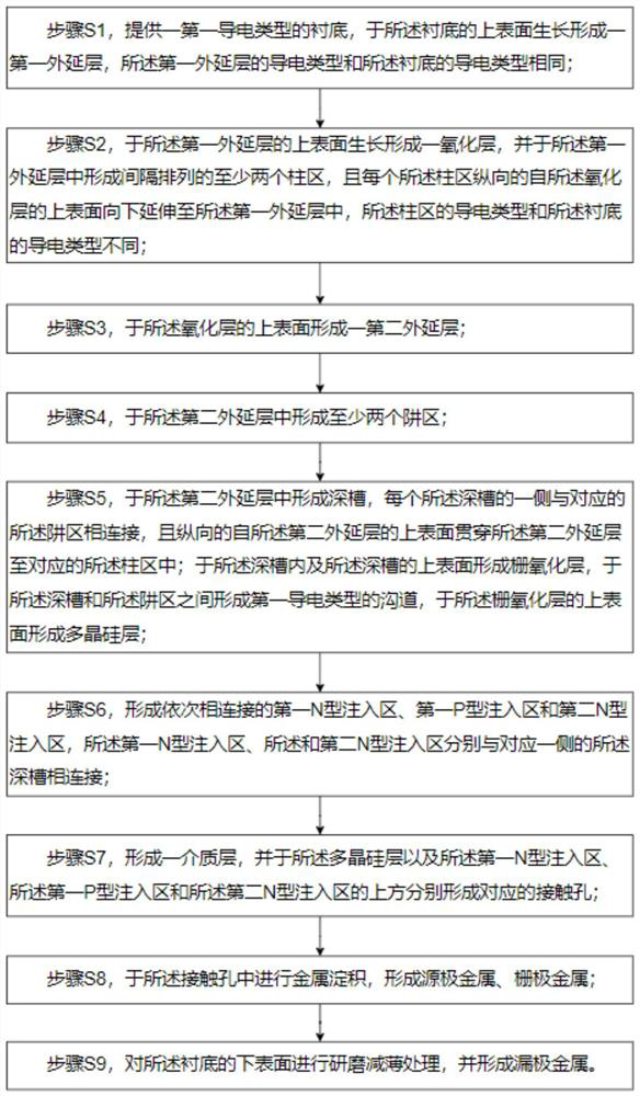
[0073] Such as figure 1 As shown, the preparation process of the exhaustive field effect transistor device is as follows:

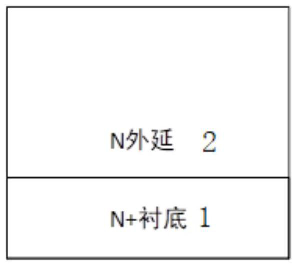
[0074] Step S1 provides a first conductivity type substrate 1, and the upper surface of the substrate 1 forms a first epitaxial layer 2, the conductivity type of the first epitaxial layer 2, and the electrically conductive type of the substrate 1 are the same;

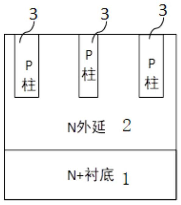
[0075] In step S1, if figure 2 As shown, first, a first conductive type silicon wafer is selected as a substrate 1, and the first conductivity type is a p-type, or the first conductivity type is n-type, preferably, the substrate 1 is N +-type substrate 1, in N + The upper surface of the substrate 1 is grown to form a first epitaxial layer 2, and the first epitaxial layer 2 is also a first conductive type, and if the substrate 1 is n-type, i.e., the first epitaxial layer 2 is also n-type.

[0076] As a preferred embodiment, the resistivity of the substrate 1 is [0.0005 Ω * cm, 0.002Ω * cm]. The electri...

Embodiment 3

[0109] Such as Figure 11 As shown, when the distance between the two deep grooves is closer, for example, when less than 10 um, then in step S2, the column region 3 formed in the first epitaxial layer 2 is two, The two column region 3 are arranged, and the two column regions 3 correspond to the position of the dark groove in the longitudinal direction, and the resulting super knot MOS device current is shorter, the on-resistance is lower, current capability More stronger, the wearing voltage is high.

[0110] The advantageous effects of the technical solution of the present invention are:

[0111] In the present invention, the gate oxide layer is disposed longitudinally, and inserted into the silicon, when the gate is not added, due to the presence of the N-channel, the current longitudinal flow, the current is shorter, and the current resistance is turned on. Lower, the current capacity is stronger; when the gate is applied, the device is turned off, the depletion zone is widen, ...


PUM

PropertyMeasurementUnit
thicknessaaaaaaaaaa
electrical resistivityaaaaaaaaaa

Abstract

The invention discloses a preparation method of a depletion mode field effect transistor device, which belongs to the field of semiconductor protection devices, and comprises the following steps: S1, forming a first epitaxial layer on a substrate; S2, growing an oxide layer, and forming at least two column regions in the first epitaxial layer; S3, forming a second epitaxial layer; S4, forming at least two well regions; S5, forming a deep groove, forming a gate oxide layer in the deep groove and on the upper surface of the deep groove, forming a channel between the deep groove and the well region, and forming a polycrystalline silicon layer on the upper surface of the gate oxide layer; S6, forming a first N-type injection region, a first P-type injection region and a second N-type injection region which are connected in sequence; S7, forming a dielectric layer, and forming a corresponding contact hole; S8, depositing source electrode metal and grid electrode metal; and S9, carrying out grinding and thinning treatment, and forming drain electrode metal. The beneficial effects of the technical scheme are that on resistance is low, withstand voltage is high during turn-off, and leakage current is small.

Description

Technical field [0001] The present invention relates to the field of semiconductor protection devices, and more particularly to a depletion type field effect transistor device and a preparation method thereof. Background technique [0002] Super-Junction Metal-Oxide Semiconductor, SJ-MOS device, by introducing a p-type and n-type semiconductor thin layer alternately arranged in the drift zone instead of the conventional single and light doped drift zone At the cutoff state, due to the mutual compensation effect due to the exhaustion field electric field in the p-type and n-type layers, the doping concentration of the P-type and the n-type layer can be made high without causing the drop of the device breakdown voltage. At the on state, high concentration doping makes its on-resistance decrease significantly. This special structure makes the super junction MOS device have advantages such as small on-resistance, fast conduction speed and low switching loss, superior performance than...

Claims


Application Information

Patent Timeline
Patent Type & Authority Applications(China)
IPC IPC(8): H01L21/336H01L29/10H01L29/423H01L29/78
CPCH01L29/1037H01L29/42364H01L29/66734H01L29/7813
Inventor 蒋骞苑赵德益吕海凤郝壮壮胡亚莉张彩霞高小丽严林彭阳
Owner SHANGHAI CHANGYUAN WAYON MICROELECTRONICS
Why Eureka
Try Eureka