Light-emitting diode chip and manufacturing method thereof

A technology for light-emitting diodes and a manufacturing method, which is applied to semiconductor devices, electrical components, circuits, etc., can solve problems such as low yield, and achieve the effects of improving yield, VF optimization, and LOP optimization.

Active Publication Date: 2017-12-26
TIANJIN SANAN OPTOELECTRONICS
View PDF6 Cites 0 Cited by
  • Summary
  • Abstract
  • Description
  • Claims
  • Application Information

AI Technical Summary

Problems solved by technology

Although the technical solution disclosed in this document solves the problem of electrode occlusion on the top surface, on the one hand, electrode alignment is required, which increases the complexity of the process, and it requires high accuracy of alignment, otherwise it is easy to cause inaccurate alignment. Causes problems such as low yield rate; on the other hand, when LOP is increased, it is accompanied by V F Becomes high

Method used


Image

  • Light-emitting diode chip and manufacturing method thereof
  • Light-emitting diode chip and manufacturing method thereof
  • Light-emitting diode chip and manufacturing method thereof

Examples


Embodiment 1

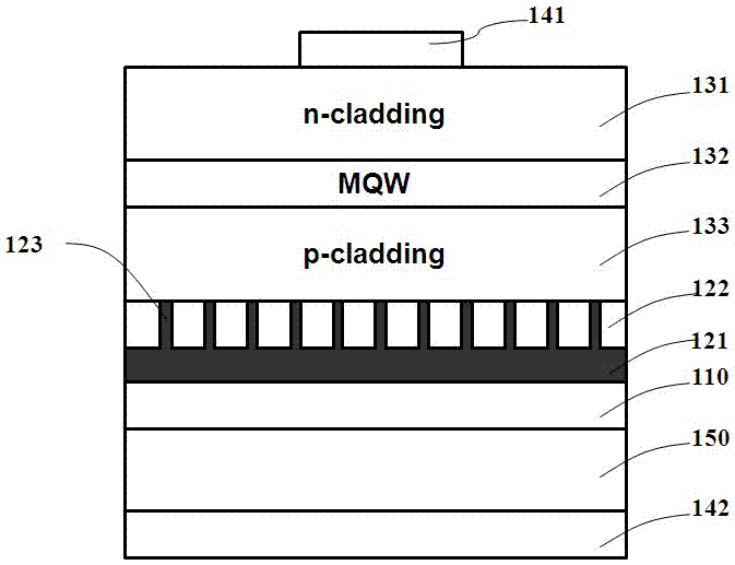
[0037] figure 1A light-emitting diode chip with a mirror system is disclosed, and its specific structure includes: a light-emitting epitaxial stack, a bonding layer 110 , a metal conductive layer 121 , a dielectric layer 122 , a first electrode 141 , a second electrode 142 and a conductive substrate 150 . Wherein, the light-emitting epitaxial stack is at least composed of a first-type semiconductor layer 131, an active layer 132 and a second-type semiconductor layer 133. When the first-type semiconductor layer 131 is a p-type semiconductor, the second-type semiconductor layer 133 can be different Electrical n-type semiconductor, on the contrary, when the first type semiconductor layer 131 is an n-type semiconductor, the second type semiconductor layer 133 can be a p-type semiconductor with different electrical properties, and the active layer 132 is located between the first type semiconductor layer 131 and the Between the second type semiconductor layers 133, there can be neu...

Embodiment 2

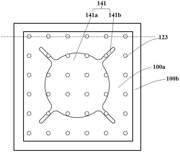
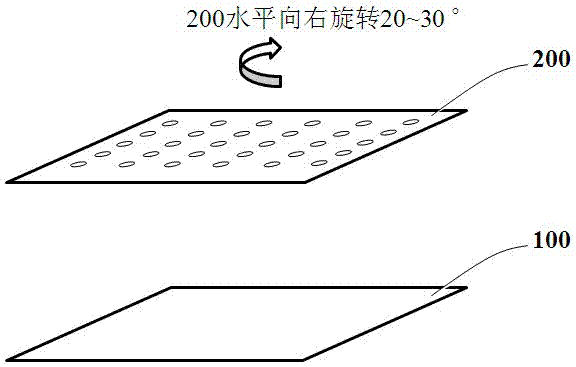
[0045] The difference between this embodiment and Embodiment 1 is that the shape of the first electrode of the LED chip is different, please refer to the attached Figure 4~5 . exist Figure 4 In the figure shown, there is no rotation angle between the conductive via array and the finger electrodes of the first electrode. There are 36 conductive vias in the light-emitting area, 8 of which are covered by the first electrode, and the effective utilization rate is 77.8%; exist Figure 5 In the figure shown, the rotation between the conductive via array and the top first electrode is 23°. There are 35 conductive vias in the light emitting area 100a, of which only 4 are completely covered by the first electrode, and the effective utilization rate reaches 88.9%. .

Embodiment 3

[0047] This embodiment discloses a method for manufacturing the light-emitting diode chip shown in the foregoing embodiments 1-2, which includes steps S100-S500, which will be described in detail below.

[0048] Step S100 : providing a light-emitting epitaxial stack, including at least a first-type semiconductor layer 131 , an active layer 132 and a second semiconductor layer 133 , which are generally formed on a growth substrate such as sapphire or gallium arsenide. The light-emitting epitaxial stack can adopt a general structure, and it is preferable that the growth substrate is easy to remove.

[0049] Step S200 : forming a dielectric layer 122 on the lower surface of the light-emitting epitaxial stack 100 , which has a conductive via array 123 . Figure 7 A specific method for this step is shown. First, a layer such as SiO is deposited on the lower surface of the light-emitting epitaxial stack 100 2 A light-transmitting insulating material layer as a dielectric layer, su...


PUM


Abstract

The present invention provides a light emitting diode chip, which comprises: a first type semiconductor layer, a second semiconductor layer and an active layer sandwiched between them; a dielectric layer located on the lower surface of the light emitting epitaxial stack, It has an array of conductive vias; a metal conductive layer is located on the lower surface of the dielectric layer, fills the conductive vias, and forms an ohmic contact with the light-emitting epitaxial stack; a conductive substrate is located on the metal conductive layer The lower surface is used to support the light-emitting epitaxial stack; the first electrode is located on the upper surface of the light-emitting epitaxial stack, including pad electrodes and finger electrodes; between the conductive via array and the finger electrodes There is a rotation angle between them, the rotation angle is selected such that a preferred number of conductive vias are not blocked by the pad electrodes and finger electrodes. The invention also provides a method for manufacturing the foregoing light-emitting diode chip.

Description

technical field [0001] The invention relates to the field of semiconductor lighting, in particular to a light-emitting diode chip and a manufacturing method thereof. Background technique [0002] In recent years, light emitting diodes (light emitting diodes, referred to as LEDs) have been widely used and play an increasingly important role in various display systems, lighting systems, automobile taillights and other fields. [0003] figure 1 An existing vertical light-emitting diode structure is shown, which uses bonding technology to convert the growth substrate into a conductive substrate with a mirror system to achieve increased brightness. In the above structure, the top electrode usually covers the conductive vias under the light-emitting epitaxial stack, so that part of the light cannot be extracted, which affects the brightness of the chip. [0004] In the prior art, in order not to overlap the top electrode and the conductive via hole below the light-emitting epita...

Claims


Application Information

Patent Timeline
Patent Type & Authority Patents(China)
IPC IPC(8): H01L33/38
CPCH01L33/387H01L2933/0016H01L33/38H01L33/405H01L31/022416
Inventor 贾月华吴俊毅谢建元
Owner TIANJIN SANAN OPTOELECTRONICS
Why Eureka
Try Eureka