Planar ultra-thin semiconductor-on-insulator channel mosfet with embedded source/drain

a semiconductor-on-insulator and channel technology, applied in the field of mosfet devices, can solve the problems of poor stress transfer to the channel, high gate-to-source-drain capacitance, loss of performance, etc., and achieve the effect of reducing overlap capacitance, reducing channel strain variations, and improving performan

Inactive Publication Date: 2007-03-29
GLOBALFOUNDRIES INC
View PDF12 Cites 39 Cited by
  • Summary
  • Abstract
  • Description
  • Claims
  • Application Information

AI Technical Summary

Benefits of technology

[0013] 1) The self-alignment eliminates variations in channel strain due to alignment tolerances between the Gate Conductor (GC) mask level and the RX mask level. The RX mask is used to define where transistors are to be formed. The GC mask is employed to define the location of the gate conductors. Note that when reference is made to the tolerance between GC and RX levels, reference is being made as to how precisely the gate conductor (GC) aligns to the edges of the regions containing the transistors (semiconductor-on-insulator body+source / drain regions.)
[0014] 2) Furthermore, gate to diffusion overlap can now be minimized, resulting in reduced overlap capacitance and higher performance.
[0015] 3) The embedded source-drain regions can now be placed much closer to the gate edge, resulting in reduced extrinsic source-drain resistance and higher performance.
[0016] B. The method uses a replacement gate process, which allows the use of a high-K / Metal gate dielectric for improved device scaling and reduced gate leakage.

Problems solved by technology

A problem encountered, particularly with semiconductor devices with Raised Source / Drain (RSD) and Ultra-Thin (UT) semiconductor-on-insulator devices is that the requirement for low raised source-drain for resistance forces the stressed liners to be located farther away from the channel than would be desired by the designer.
The loss of performance due to the inefficient transfer of stress to the channel is compounded by the competing need to use sidewall insulating spacers which are as thick as possible, to minimize gate to source-drain capacitance.
The embodiment of Hsu et al. is an example of the above described problem that it has high gate to source-drain capacitance and poor stress transfer to the channel.
To avoid high gate to source-drain capacitance very thick sidewall spacers are used, which results in very poor stress transfer if an overlying stress liner is used.
Chen et al. does not teach the use of porous silicon to form BOX regions.
The semiconductor under the gate is bulk and therefore suffers from the short channel scaling problems that our UTSOI structure solves.

Method used


Image

  • Planar ultra-thin semiconductor-on-insulator channel mosfet with embedded source/drain
  • Planar ultra-thin semiconductor-on-insulator channel mosfet with embedded source/drain
  • Planar ultra-thin semiconductor-on-insulator channel mosfet with embedded source/drain

Examples


first embodiment

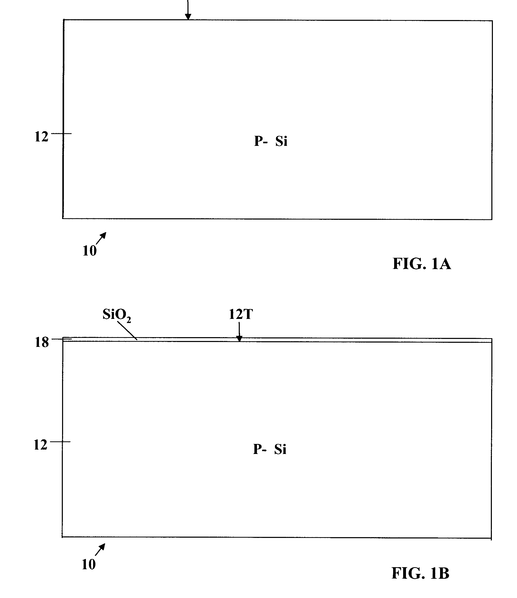
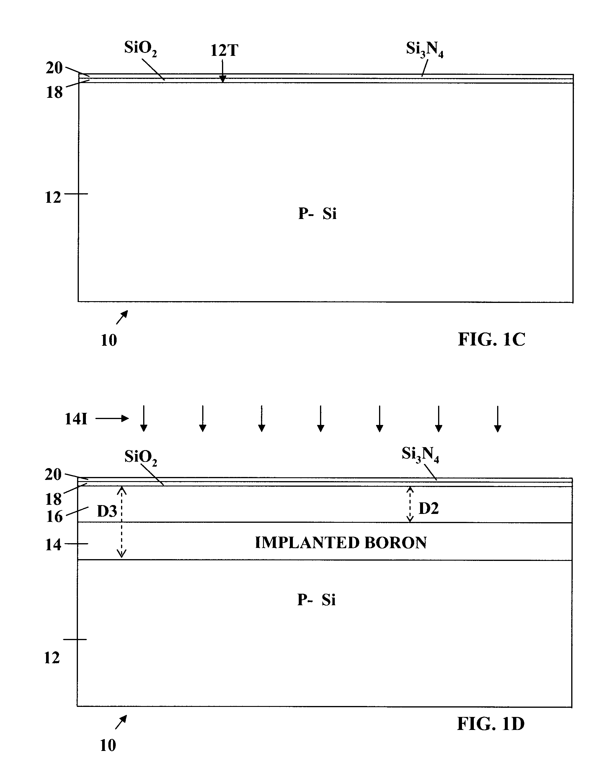
[0029]FIG. 1A shows a sectional view of a device 10 in accordance with this invention in an early stage of fabrication in accordance with step A of FIG. 3. The method begins preferably with a substrate 12 composed of conventional bulk semiconductor material selected from group IV periodic table elements and compound semiconductors from groups III-V and II-VI. For example silicon, germanium, silicon-germanium, and silicon-carbide are group IV periodic table elements which may be employed. Compound semiconductors from groups III-V and II-VI include such materials as GaAs, InP, and AlGaAs.

[0030] The semiconductor substrate 12 may comprise a thick portion under all the BOX regions of a first semiconductor.

[0031] Preferably the substrate 16 that can be formed by epitaxial growth of an upper, second semiconductor region on a substrate composed of a first semiconductor region 12. That is to say that one starts with a laminated semiconductor substrate which does not initially contain a bu...

second embodiment

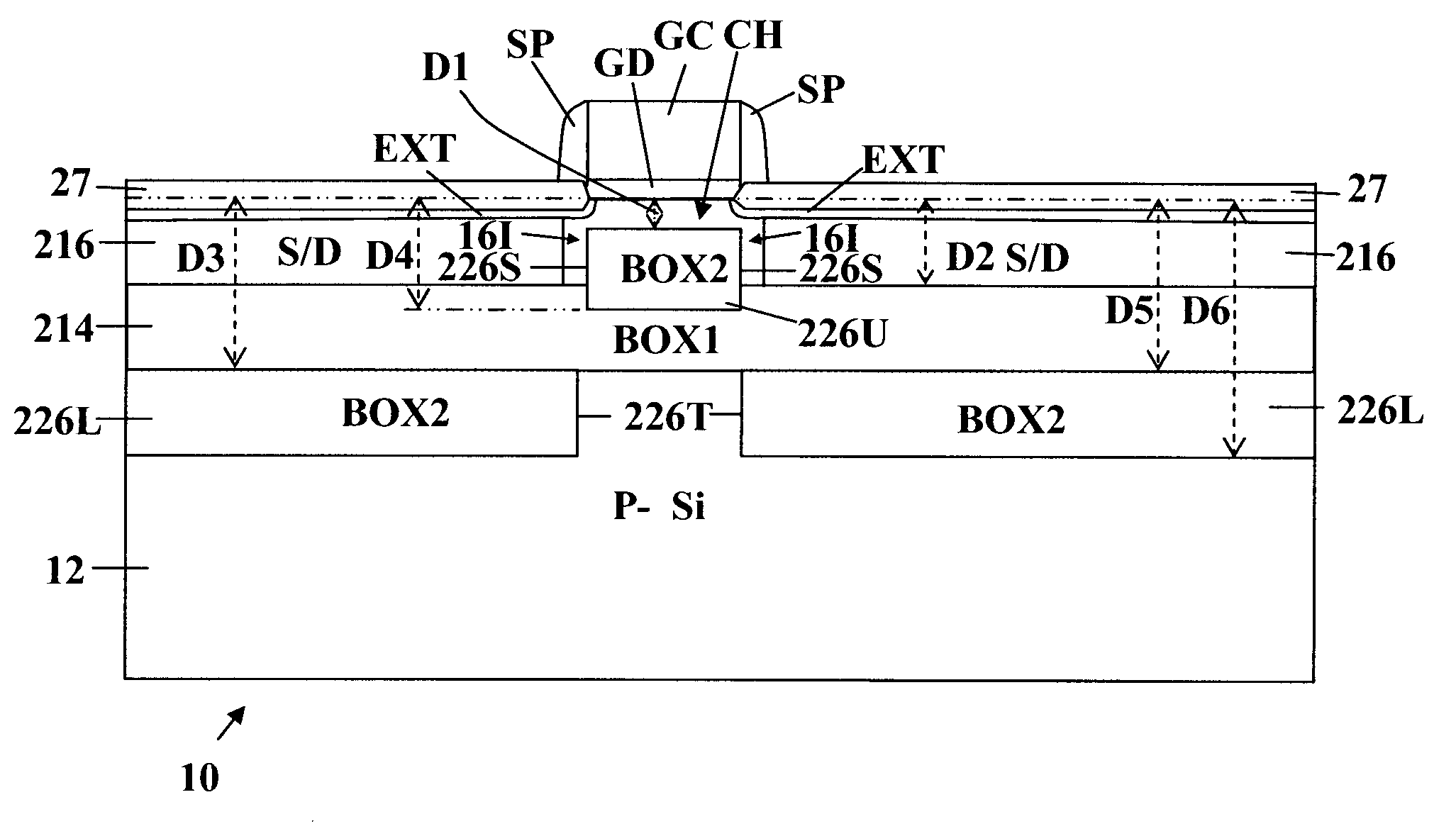
[0064]FIG. 2 shows a second embodiment of this invention comprising a device 100 which is similar to the device 10 of FIG. 1W, but which has been modified by the formation of the structure on a BOX substrate 11 as compared with the bulk substrate 11 of FIGS. 1A-1W. In addition, the lower BOX regions 226L are shown overlapping the BOX1 region 214 so that the depth D5 of the top surface of the lower BOX regions 226L is less than the depth D3 of the top surface of the BOX1 region 214. The device 100 can be manufactured in accordance with the steps shown in FIG. 3.


PUM


Abstract

A MOSFET structure includes a planar semiconductor substrate, a gate dielectric and a gate. An ultra-thin (UT) semiconductor-on-insulator channel extends to a first depth below the top surface of the substrate and is self-aligned to and is laterally coextensive with the gate. Source-drain regions, extend to a second depth greater than the first depth below the top surface, and are self-aligned to the UT channel region. A first BOX region extends across the entire structure, and vertically from the second depth to a third depth below the top surface. An upper portion of a second BOX region under the UT channel region is self-aligned to and is laterally coextensive with the gate, and extends vertically from the first depth to a third depth below the top surface, and where the third depth is greater than the second depth.

Description

BACKGROUND OF THE INVENTION [0001] This invention relates to MOSFET devices and more particularly to Ultra Thin (UT) SEMiconductor-On-Insulator (SEMOI) channel MOSFET devices with the source and drain regions formed in thicker SOI regions of a semiconductor substrate. As employed herein the term SEMiconductor-On-Insulator (SEMOI) is a generic term which refers generally to structures of a semiconductor layer formed on an insulator such Silicon-On-Insulator (SOI), Silicon-Germanium-On-lnsulator (SGOI), and Germanium-On-Insulator (GOI) structures. [0002] A problem encountered, particularly with semiconductor devices with Raised Source / Drain (RSD) and Ultra-Thin (UT) semiconductor-on-insulator devices is that the requirement for low raised source-drain for resistance forces the stressed liners to be located farther away from the channel than would be desired by the designer. For example a UT semiconductor-on-insulator device with an RSD of 30 nm (including silicide) encounters a signif...

Claims


Application Information

Patent Timeline
Patent Type & Authority Applications(United States)
IPC IPC(8): H01L29/94
CPCH01L21/02203H01L21/02238H01L21/02255H01L21/02299H01L29/7833H01L21/31662H01L29/1083H01L29/66545H01L29/6659H01L21/2652
Inventor CHENG, KANGGUOCHIDAMBARRAO, DURESETIGREENE, BRIAN JOSEPHMANDELMAN, JACK A.RIM, KERN
Owner GLOBALFOUNDRIES INC
Why Eureka
Try Eureka