Apparatus and method for reducing parasitic capacitance in a semiconductor device

a semiconductor device and parasitic capacitance technology, applied in semiconductor devices, semiconductor/solid-state device details, oscillators, etc., can solve the problems of invariably introducing inaccuracies in the vco, negatively affecting the reliability, performance and power consumption of the device, and being more sensitive to signal propagation delays

Active Publication Date: 2007-03-29
AVAGO TECH INT SALES PTE LTD
View PDF2 Cites 0 Cited by
  • Summary
  • Abstract
  • Description
  • Claims
  • Application Information

AI Technical Summary

Problems solved by technology

This is especially critical in high frequency application, as phase noise and jitters are more prevalent and detrimental to the performance of the VCO.
Even though a VCO could be optimally designed for a specific high frequency application, manufacturing process tolerances will invariably introduce inaccuracies into the VCO.
These parasitic components negatively effect the reliability, performance, and power consumption of the device.
But as a semiconductor device gets progressively smaller it becomes more sensitive to signal propagation delays caused by parasitic resistance and capacitance inherent to the interconnection lines within the device.
A wider interconnection line could be used to ease this problem; however, this will increase the parasitic capacitance of the line to the ground.

Method used


Image

  • Apparatus and method for reducing parasitic capacitance in a semiconductor device
  • Apparatus and method for reducing parasitic capacitance in a semiconductor device
  • Apparatus and method for reducing parasitic capacitance in a semiconductor device

Examples


Embodiment Construction

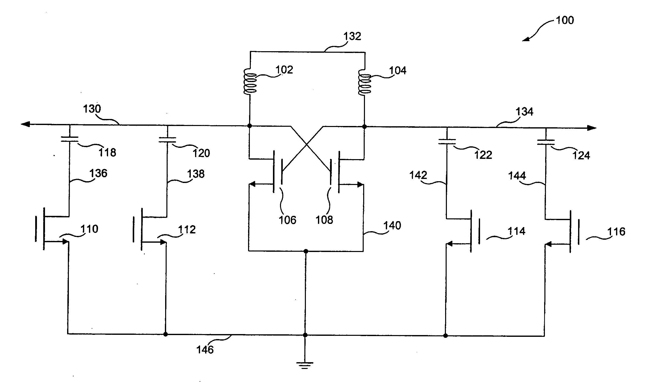
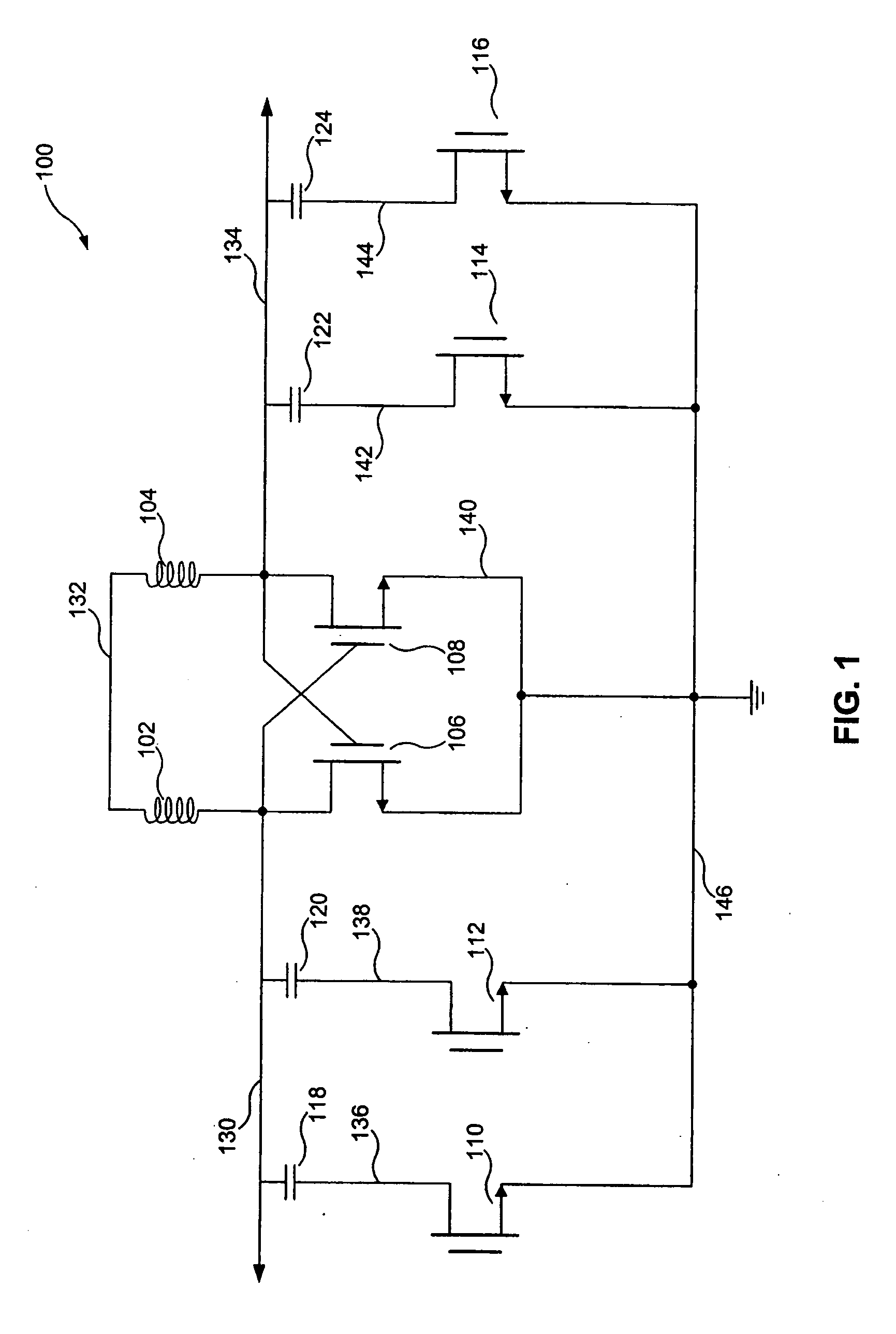
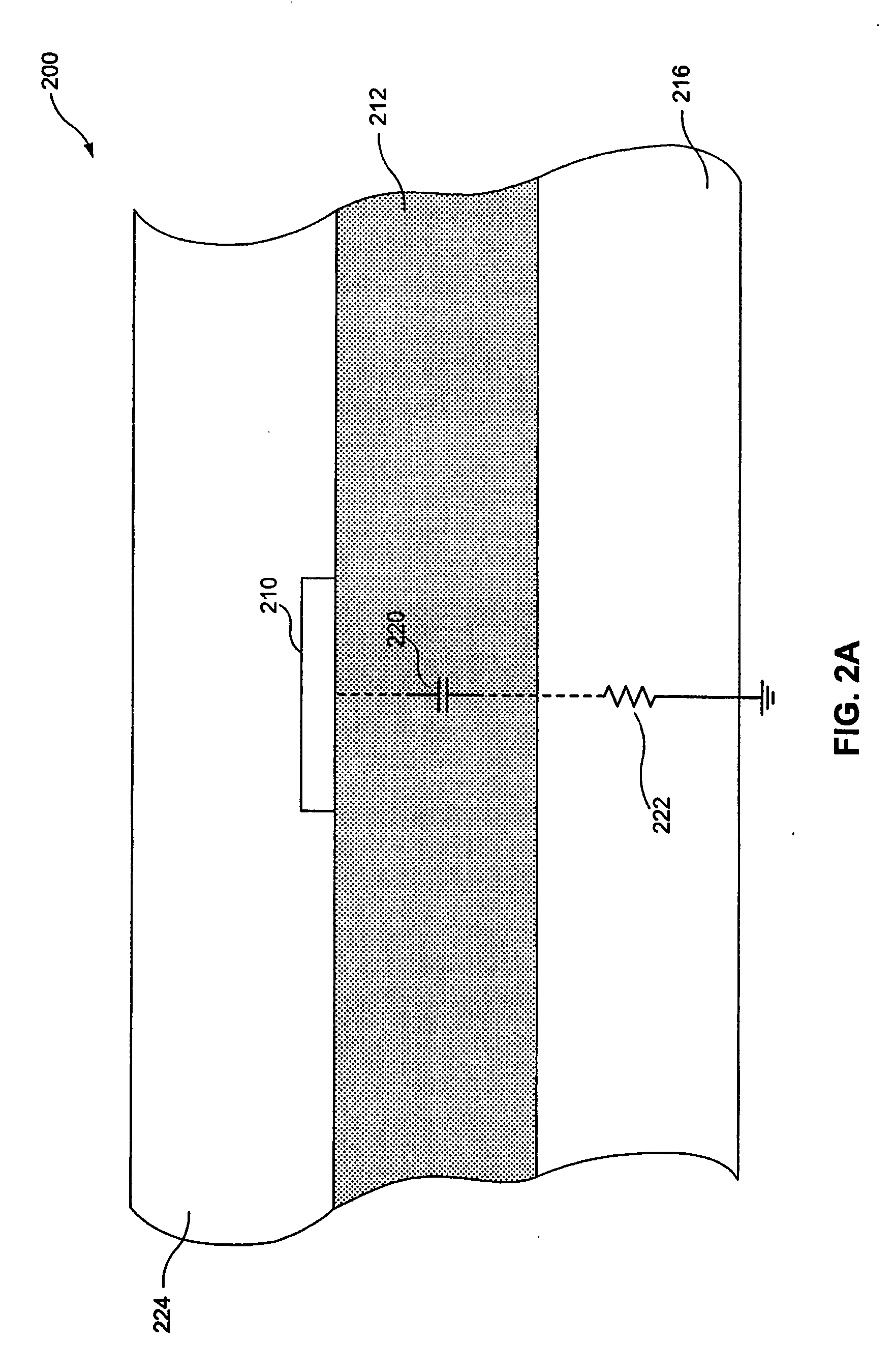
[0017] This specification discloses one or more embodiments that incorporate the features of this invention. The embodiment(s) described, and references in the specification to “one embodiment”, “an embodiment”, “an example embodiment”, etc., indicate that the embodiment(s) described may include a particular feature, structure, or characteristic, but every embodiment may not necessarily include the particular feature, structure, or characteristic. Moreover, such phrases are not necessarily referring to the same embodiment. Further, when a particular feature, structure, or characteristic is described in connection with an embodiment, it is understood that it is within the knowledge of one skilled in the art to effect such feature, structure, or characteristic in connection with other embodiments whether or not explicitly described.

[0018] An embodiment of the present invention is now described. While specific methods and configurations are discussed, it should be understood that this...


PUM


Abstract

A semiconductor device exhibiting low parasitic resistance comprises a first substrate characterized by a first resistivity; a second substrate characterized by a second resistivity, a third substrate and a metal element. These substrates form a multi-layer semiconductor device where the second substrate is formed on the first substrate; the third substrate is formed on the second substrate; and the metal element is formed on the third substrate. The second substrate is electrically grounded and is highly doped with acceptor dopant as compared to the first substrate. In this way, the second resistivity is lower than the first resistivity.

Description

CROSS-REFERENCE TO RELATED APPLICATIONS [0001] This application claims priority to U.S. Provisional Application No. 60 / 720,653, filed Sep. 27, 2005, entitled “Apparatus and Method for Reducing Parasitic Capacitance in a Semiconductor Device,” incorporated herein by reference in its entirety.BACKGROUND OF THE INVENTION [0002] As wireless devices are becoming increasing faster and smaller, the power consumption, reliability, and performance of a voltage controlled oscillator (VCO) in such devices have become a design focus. A VCO is typically used in modulating and demodulating a radio frequency (RF) signal by mixing the un-modulated or modulated signal with a locally generated oscillating signal. For example, when demodulating a RF signal, it is important to accurately match the VCO's generated oscillating signal with the RF's carrier signal. This is especially critical in high frequency application, as phase noise and jitters are more prevalent and detrimental to the performance of ...

Claims


Application Information

Patent Timeline
Patent Type & Authority Applications(United States)
IPC IPC(8): H01L29/00
CPCH03B5/1228H03B5/1265H03B5/1212
Inventor CHIEN, HUNG-MING
Owner AVAGO TECH INT SALES PTE LTD
Why Eureka
Try Eureka