Phase locked loop having reduced inherent noise
- Summary
- Abstract
- Description
- Claims
- Application Information
AI Technical Summary
Benefits of technology
Problems solved by technology
Method used
Image

Examples
Embodiment Construction
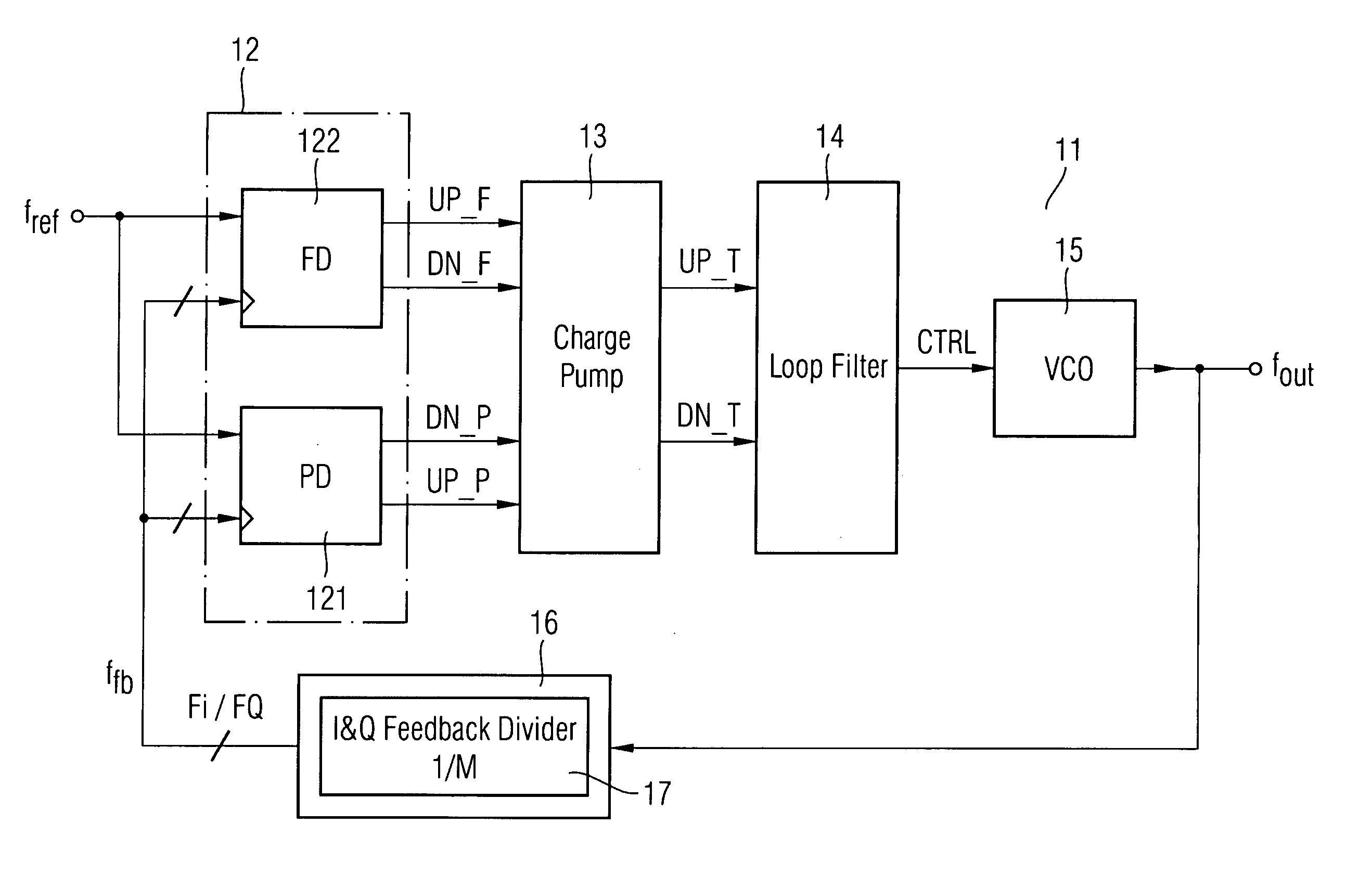
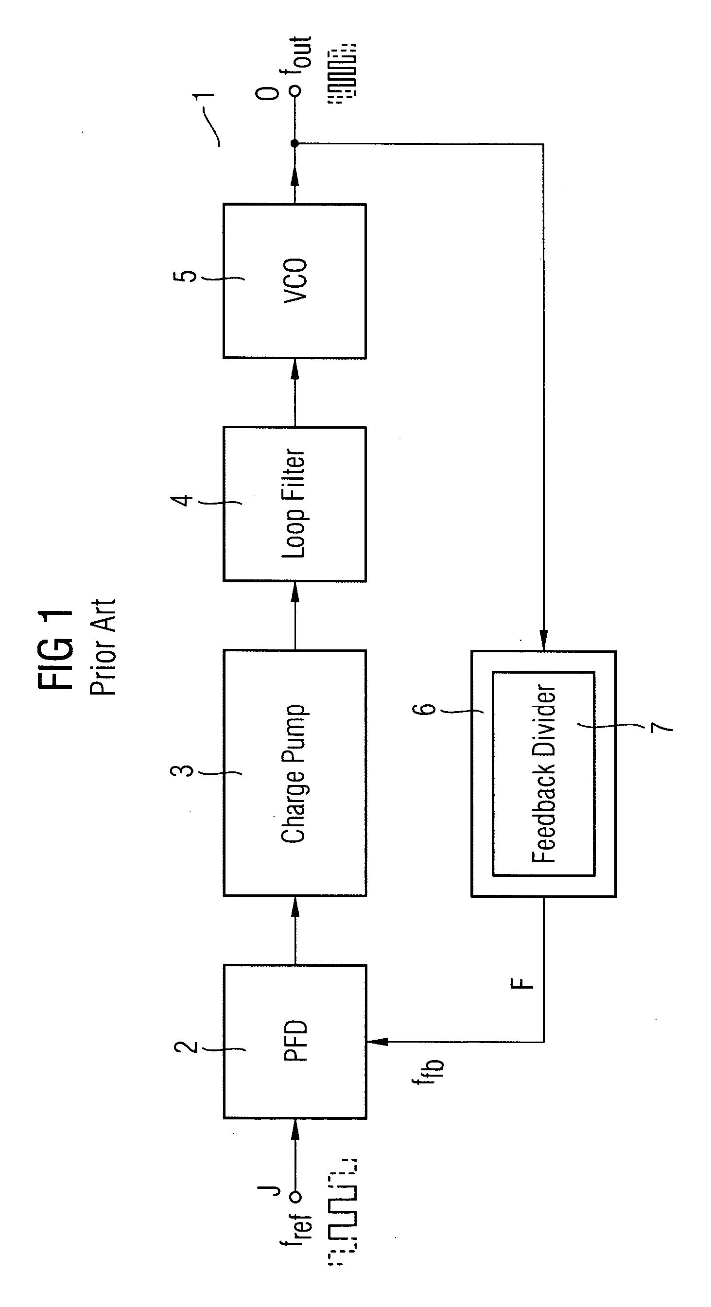
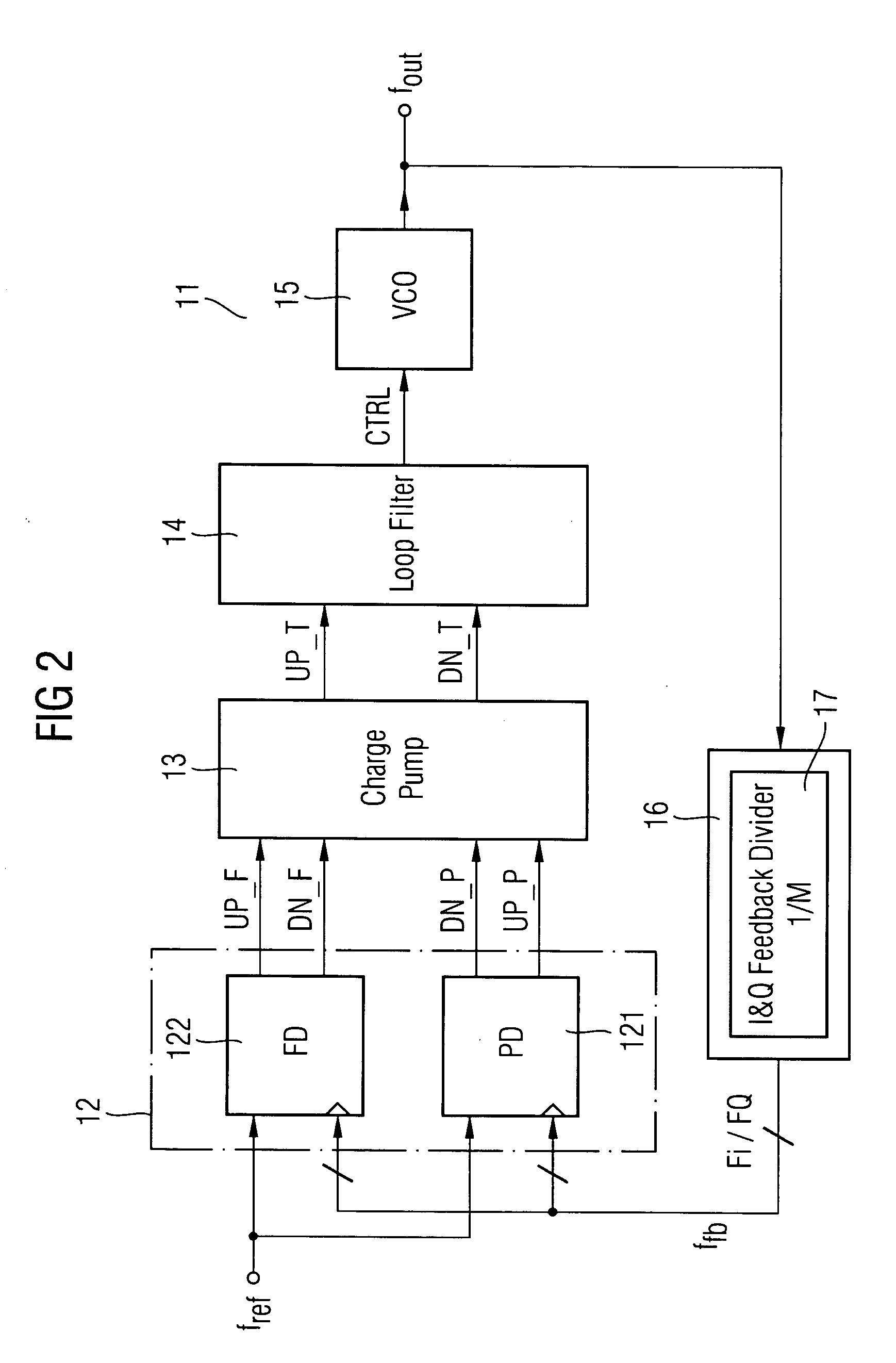
[0053] In FIG. 1, a block diagram of an analog phase locked loop circuit 1 is depicted. The phase locked loop circuit 1 comprises a frequency / phase detector (FPD) 2 which receives an input signal 1 having an input frequency fref and a feedback signal F having a feedback frequency ffb. The frequency / phase detector 2 compares the input signal I and the feedback signal F and supplies a leading / lagging information to a charge pump circuit 3. The charge pump 3 transforms the leading / lagging information to current pulses which are provided via a loop filter 4 to a voltage controlled oscillator 5 which provides an output signal O having a frequency IOUT. The output of the voltage controlled oscillator 5 is coupled to a feedback loop, and the output of the feedback loop provides the feedback signal F supplied to the respective input of the frequency / phase detector 2 as mentioned above.
[0054] Such a phase locked loop circuit is known in the art and provides an output signal u having a frequ...
PUM
 Abstract
Description
Claims
Application Information