Printed circuit board and manufacturing method thereof

a technology of printed circuit board and manufacturing method, which is applied in the direction of printed circuit aspects, printed circuit non-printed electric components association, printed circuit non-printed electric components incorporation, etc., can solve the problems of affecting yield, increasing manufacturing costs, and the stiffness and heat-releasing property of the substrate itself remain unchanged, so as to improve the stiffness and heat-releasing property of the core member, improve the adhesion, and stabilize the embedding of the electronic component.

Inactive Publication Date: 2007-04-05
SAMSUNG ELECTRO MECHANICS CO LTD
View PDF8 Cites 72 Cited by
  • Summary
  • Abstract
  • Description
  • Claims
  • Application Information

AI Technical Summary

Benefits of technology

[0010] The present invention aims to provide a printed circuit board and manufacturing method thereof, for embedding an electronic component in a core member, which improve the stiffn

Problems solved by technology

However, in a conventional printed circuit board having embedded electronic components, there is a high probability that problems in heat release due to embedding electronic components such as high-density IC's, or problems such as delamination, etc., will affect the yield, and there are difficulties in the overall p

Method used


Image

  • Printed circuit board and manufacturing method thereof
  • Printed circuit board and manufacturing method thereof
  • Printed circuit board and manufacturing method thereof

Examples


Embodiment Construction

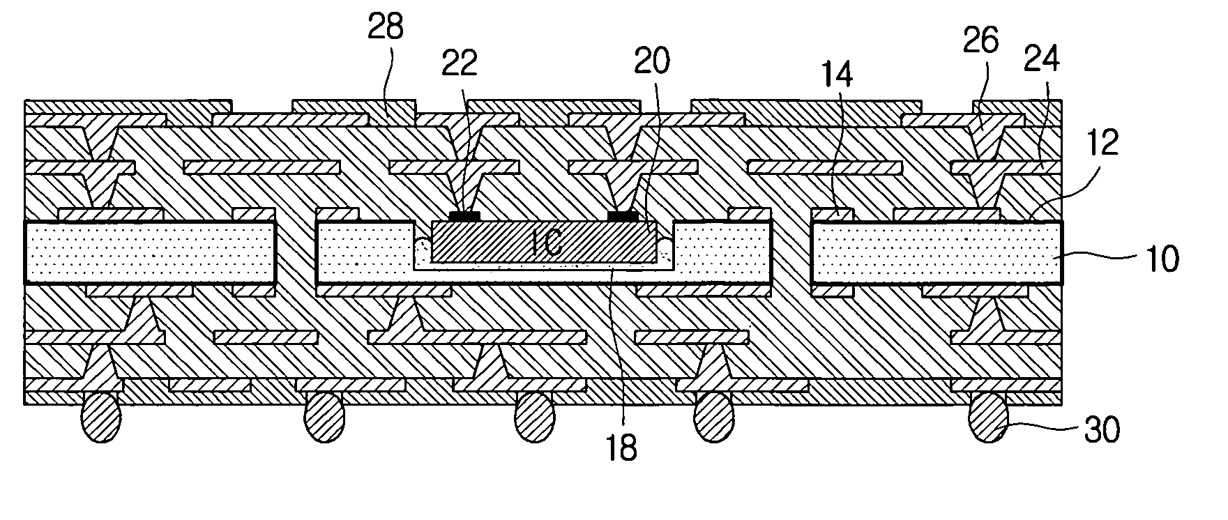
[0026] Embodiments of the printed circuit board and manufacturing method thereof according to the present invention will be described below in more detail with reference to the accompanying drawings. In the description with reference to the accompanying drawings, those components are rendered the same reference number that are the same or are in correspondence regardless of the figure number, and redundant explanations are omitted.

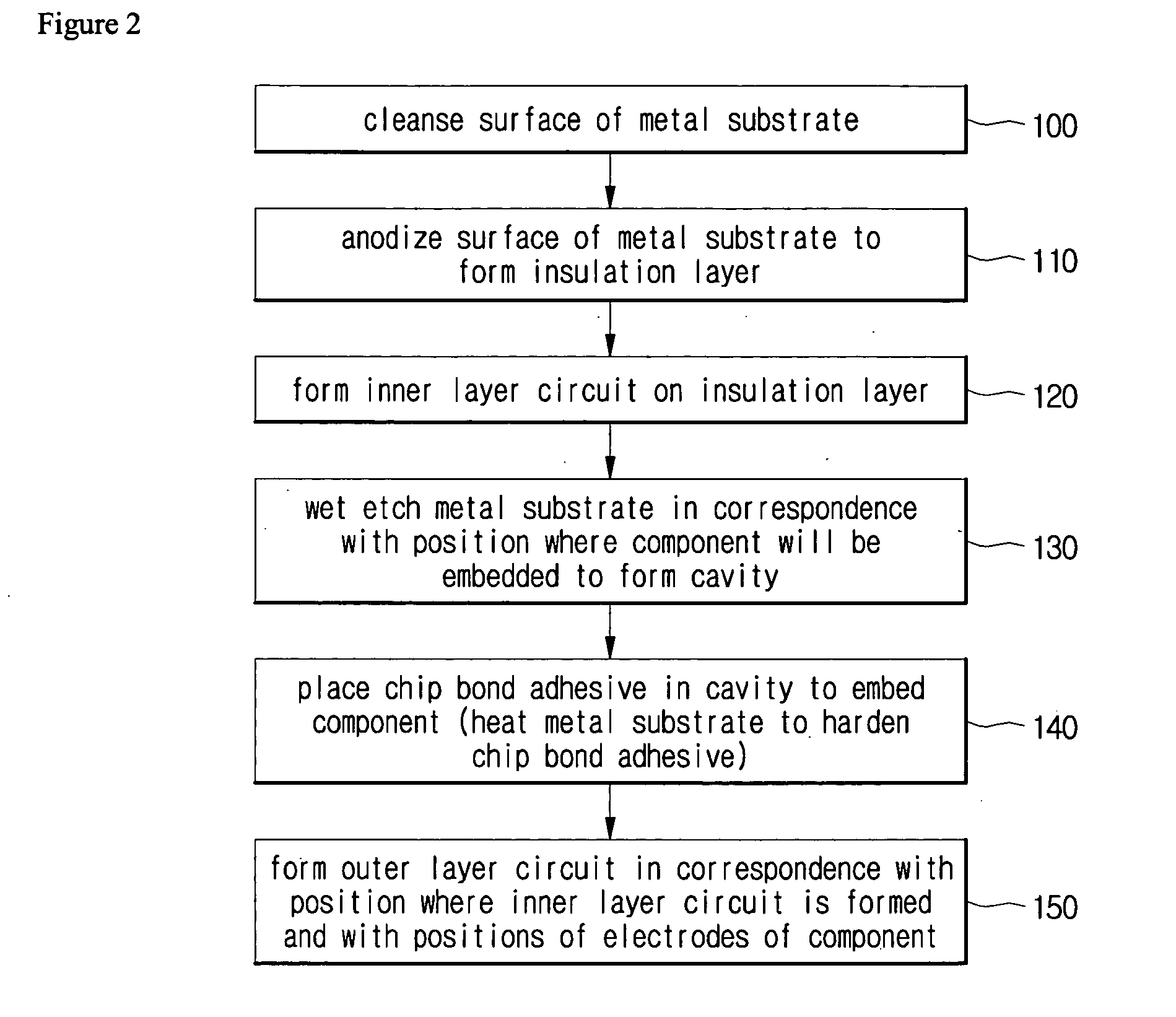
[0027]FIG. 2 is a flowchart illustrating a method of manufacturing a printed circuit board having an embedded electronic component according to an embodiment of the present invention.

[0028] The present invention is characterized by using a metal substrate as a core member, so as to minimize the adding of new members to a method of manufacturing a conventional printed circuit board, maintain stiffness even with a lower thickness, and promote high efficiency in heat-releasing property.

[0029] In order to implement such a structure, the printed circuit boar...


PUM

PropertyMeasurementUnit
Thixotropic indexaaaaaaaaaa
aaaaaaaaaa

Abstract

A printed circuit board and manufacturing method thereof are disclosed. By use of a method of manufacturing a printed circuit board, which uses a metal substrate as a core member and has an electronic component embedded in the metal substrate, mainly comprising: (a) anodizing at least one surface of the metal substrate to form at least one insulation layer, (b) forming an inner layer circuit on the at least one insulation layer, (d) placing chip bond adhesive in correspondence with a position where the electronic component is to be embedded and mounting the electronic component, and (e) forming an outer layer circuit in correspondence with a position where the inner layer circuit is formed and with positions of the electrodes of the electronic component, and which may further comprise an operation (c) of etching the metal substrate to form a cavity in correspondence with a position where the electronic component is to be embedded between the operations (b) and (d), a metal substrate, such as that of aluminum, etc., is rendered electrically insulating by applying an anodizing process and is used as a core member in a printed circuit board, so that bending stiffness and heat-releasing property are improved; wet etching can be applied, so that manufacturing costs are reduced; and a chip bond adhesive, die attach film, or nonconductive paste, etc., that is high in thixotropy is used in embedding the electronic component, so that the degree of precision may be increased for the position and height of the electronic component when embedding the electronic component.

Description

CROSS-REFERENCE TO RELATED APPLICATIONS [0001] This application claims the benefit of Korean Patent Application No. 2005-0093109 filed with the Korean Intellectual Property Office on Oct. 4, 2005, the disclosure of which is incorporated herein by reference in its entirety. BACKGROUND [0002] 1. Technical Field [0003] The present invention relates to a printed circuit board, more particularly to a printed circuit board having an embedded electronic component and manufacturing method thereof. [0004] 2. Description of the Related Art [0005] As a part of next-generation multi-functional miniature package technology, attention is being focused on the development of a printed circuit board having embedded electronic components. Along with the advantages of multi-functionality and miniaturization, a printed circuit board having embedded electronic components also allows, to a degree, more sophisticated functionalities, as the wiring distance can be minimized in a high-frequency range of 100...

Claims


Application Information

Patent Timeline
IPC IPC(8): H05K1/16
CPCH01L23/13Y10T29/49156H01L23/5389H01L24/19H01L24/24H01L2224/04105H01L2224/20H01L2224/24227H01L2224/73267H01L2224/83192H01L2224/92244H01L2924/01005H01L2924/01012H01L2924/01013H01L2924/01015H01L2924/01029H01L2924/01033H01L2924/01078H01L2924/14H01L2924/15153H01L2924/15165H01L2924/15311H05K1/021H05K1/053H05K1/185H05K3/4608H05K2201/09745H05K2201/10477H05K2201/10674H05K2203/0315H01L23/142H01L2924/07802H01L2924/01006H01L2224/32245H01L2224/32225H01L2924/00H01L2924/181H05K1/18H05K3/30
Inventor LEE, DOO-HWANYOO, JE-GWANGKIM, SEUNG-GULEE, JAE-KULKIM, MOON-ILKIM, HYUNG-TAE
Owner SAMSUNG ELECTRO MECHANICS CO LTD
Why Eureka
Try Eureka