Method for improving via's impedance

a technology of impedance and via, which is applied in the direction of program control, high frequency circuit adaptation, instruments, etc., can solve the problems of affecting the integrity of signals, affecting the signal, and affecting the transmission line and the via connection portion

Inactive Publication Date: 2007-04-05
HONG FU JIN PRECISION IND (SHENZHEN) CO LTD +1
View PDF20 Cites 25 Cited by
  • Summary
  • Abstract
  • Description
  • Claims
  • Application Information

AI Technical Summary

Problems solved by technology

As reduction in size and increase in transmission signal frequency of this multilayer circuit substrate have been needed, a transmission loss due to signal wave reflection in the transmission lines and via connecting portion have become a more serious problem.
These may harm ...

Method used


Image

  • Method for improving via's impedance
  • Method for improving via's impedance
  • Method for improving via's impedance

Examples


Embodiment Construction

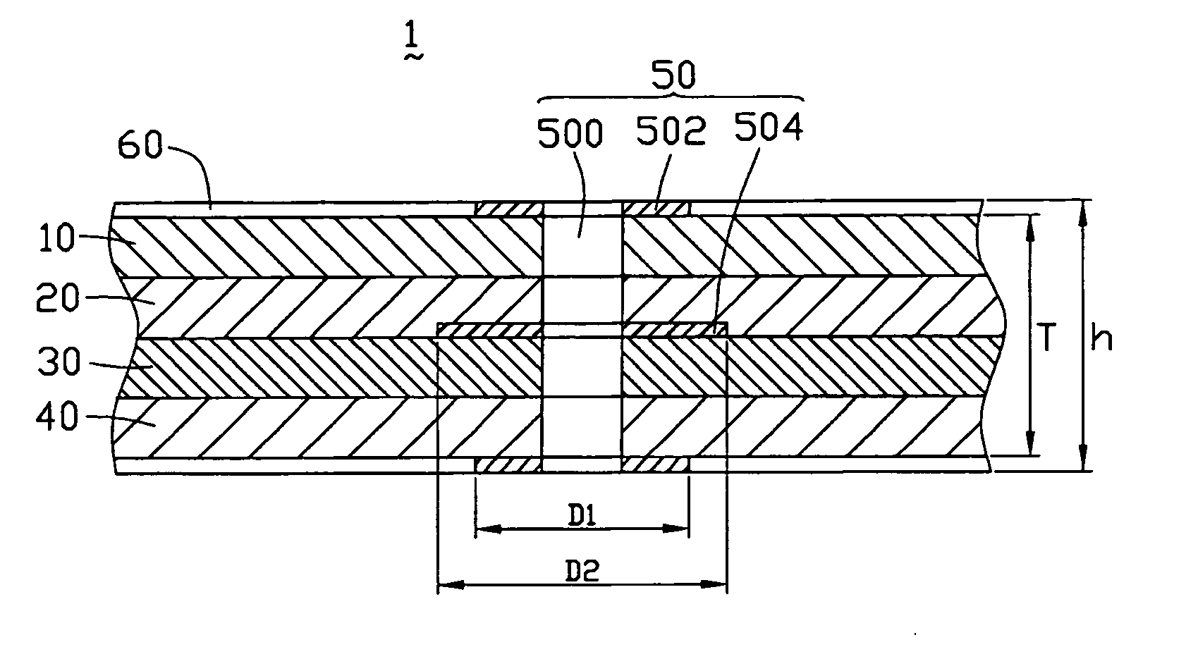
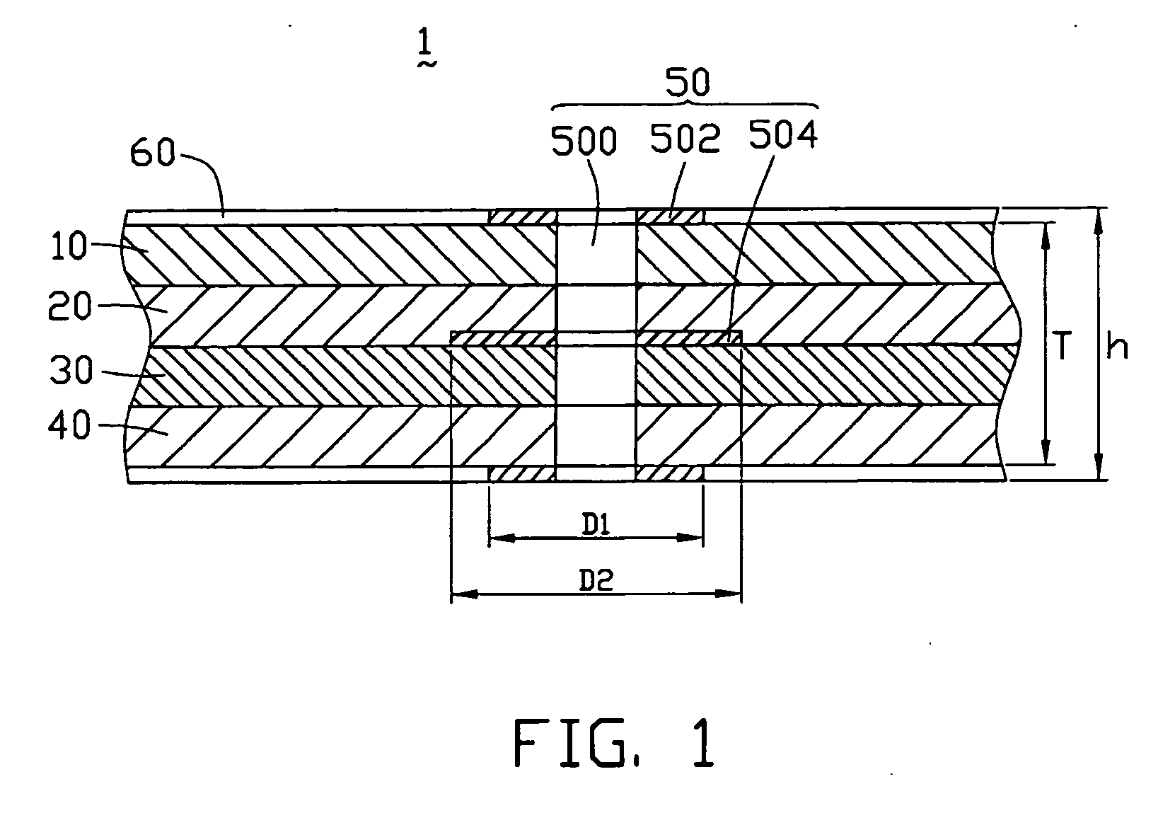
[0010] Referring to FIG. 1, a PCB (printed circuit board) 1 includes a first signal layer 10, a power layer 20, a ground layer 30, and a second signal layer 40, one below another in turn. A via 50 is defined throughout the PCB board 1. Traces 60 are separately arranged on the first signal layer 10 and the second layer 40. The via 50 includes a drill hole 500. A pair of pads 502 is formed encircling ends of the drill hole 500, connecting the traces 60 to the via 50, and respectively contacting the first signal layer 10 and the second signal layer 40. An anti-pad 504 is formed encircling a middle portion of the drill hole 500 and sandwiched between the ground layer 30 and the power layer 20.

[0011] An impedance of the via 50 is Z, a stray capacitance of the via 50 is Cj, and a parasitic inductance of the via 50 is Lj. The stray capacitance CJ may delay a rising time of signals and decrease a transmitting speed of signal. The parasitic inductance Lj may weaken shunt capacitors mounted ...


PUM


Abstract

A method is for controlling an impedance of a via of a printed circuit board. The Via is connected with a trace and includes a drill hole, a pad and an anti-pad. The method includes steps of: building a math model; testing whether an impedance of the via matching with an impedance of the trace; analyzing the impedance of the via if passing the testing; and adjusting parameters of the pad, the anti-pad, and the drill hole if fails testing, and returning to the simulating step, till impedance matching achieved. The method which can efficiently keep signals integrality and increase signal transmission speed.

Description

BACKGROUND OF THE INVENTION [0001] 1. Field of the Invention [0002] The present invention relates to a method of controlling impedance of vias, and more particularly to a method of controlling impedance of vias for efficiently maintaining signal integrity and increasing signal transmission speed. [0003] 2. General Background [0004] Conventionally, there has been a high-frequency multilayer circuit substrate, in which transmission lines are connected by way of vias provided for the improvement in performance of a high-frequency circuit and for high-density mounting. As reduction in size and increase in transmission signal frequency of this multilayer circuit substrate have been needed, a transmission loss due to signal wave reflection in the transmission lines and via connecting portion have become a more serious problem. These may harm integrity of the signals. Stray capacitance and parasitic inductance of the vias always exist. The stray capacitance may delay a rising time of the s...

Claims


Application Information

Patent Timeline
IPC IPC(8): H05K1/11H01R12/04
CPCG06F17/5068H05K1/0237H05K1/116H05K3/0005H05K3/0047H05K3/429H05K2201/09718H05K2203/163G06F30/39
Inventor LIN, YU-HSUYEH, SHANG-TSANGLI, CHUAN-BING
Owner HONG FU JIN PRECISION IND (SHENZHEN) CO LTD
Why Eureka
Try Eureka