Processing method of wafer

a processing method and technology of a wafer, applied in the field of processing methods of a wafer, can solve the problems of difficult to stably hold the semiconductor wafer, difficult to handle the semiconductor wafer, and easy cracking of the semiconductor wafer, so as to prevent the increase of costs and enhance the process for obtaining a plurality of devices from a wafer having an outer peripheral surplus region around the device region

Active Publication Date: 2007-04-05
DISCO CORP
View PDF6 Cites 23 Cited by
  • Summary
  • Abstract
  • Description
  • Claims
  • Application Information

AI Technical Summary

Benefits of technology

[0015] According to the invention, the efficiency of the process for obtaining a plurality of devices from a wafer having an outer peripheral surplus region ...

Problems solved by technology

If the semiconductor wafer is thinned, however, its rigidity is deteriorated, and there is a problem that it becomes difficult to handle the semiconductor wafer and the semiconductor wafer is easily cracked.
Here, if the semiconductor wafer is a flat plate, its entire back surface comes into intimate contact with the chuck t...

Method used


Image

  • Processing method of wafer
  • Processing method of wafer
  • Processing method of wafer

Examples


first embodiment

[1] Processing Method of the First Embodiment

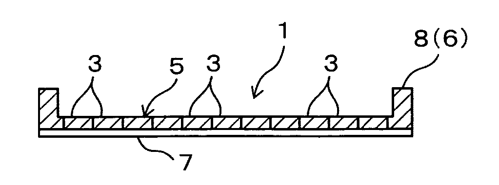
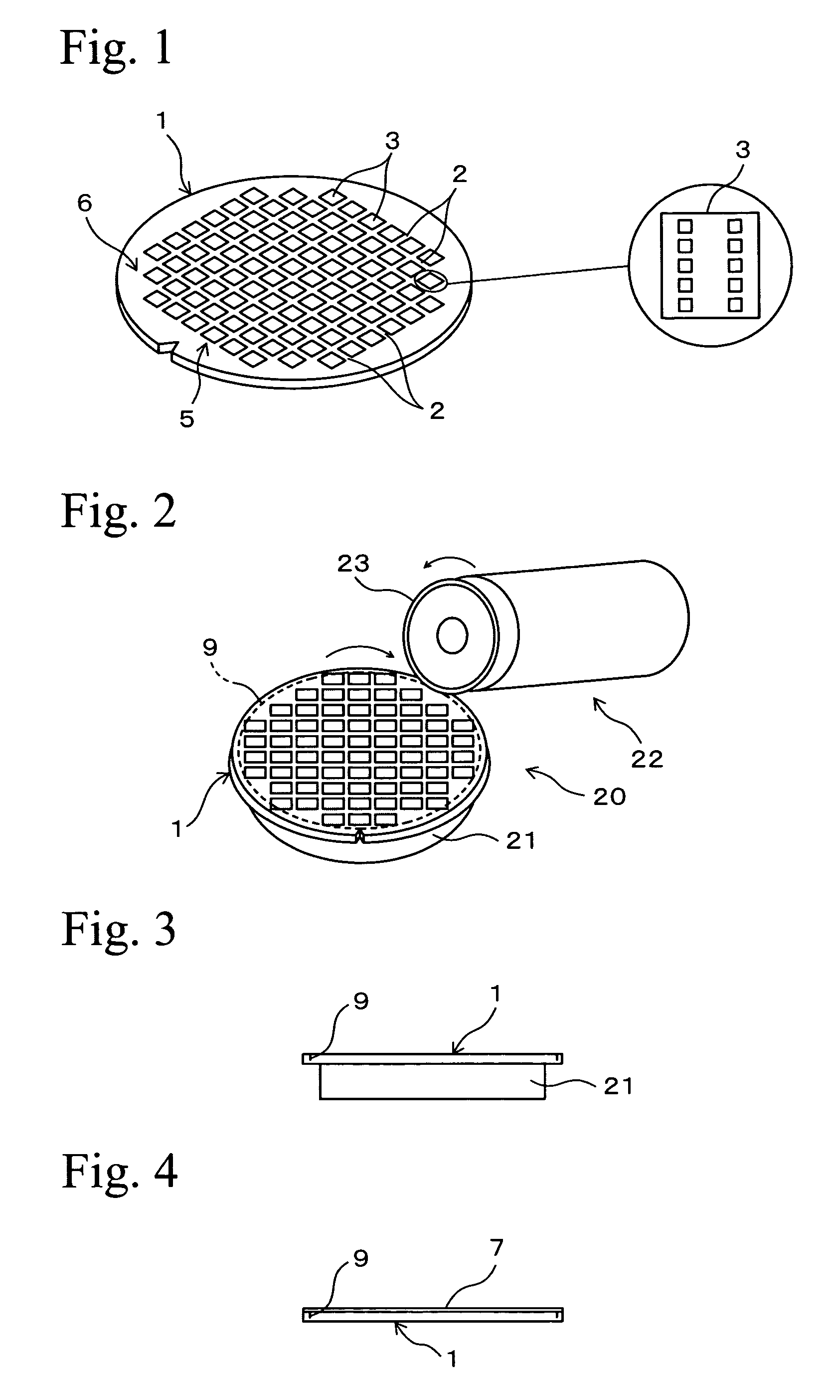
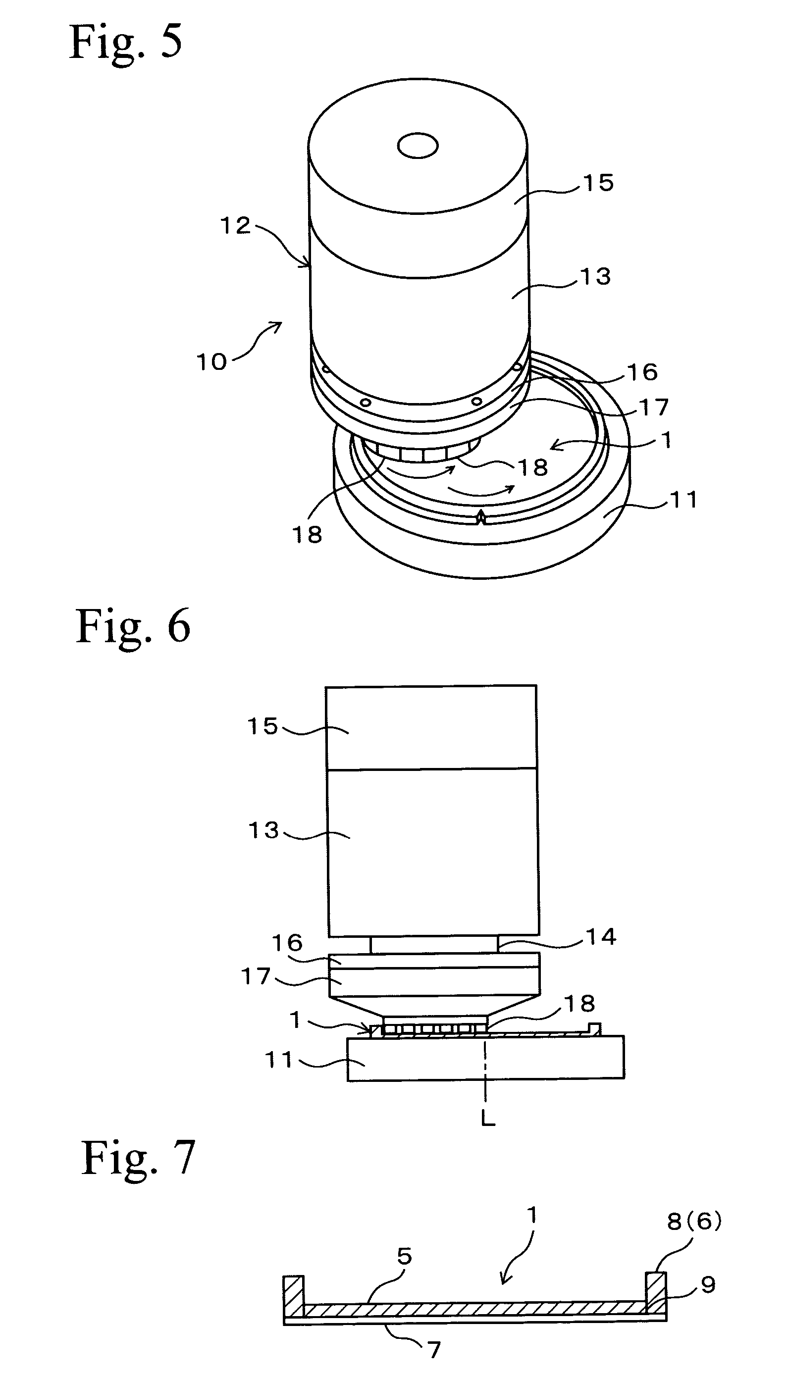
[0037] Reference numeral 1 in FIG. 1 shows a disk-like semiconductor wafer (hereinafter referred to simply as “wafer”) such a silicon wafer. The thickness of the wafer 1 before it is processed is about 700 μm, and rectangular semiconductor chips 3 are defined by lattice streets 2. Electronic circuits are formed on front surfaces of the semiconductor chips 3. A region where the plurality of semiconductor chips 3 are formed is a substantially circular device region 5 which is coaxial with the wafer 1. An annular outer peripheral surplus region 6 exists around the device region 5.

[0038] This embodiment is a method in which a portion of a back surface of the wafer 1 corresponding to the device region 5 is ground, this portion is thinned to a necessary thickness, and respective semiconductor chips 3 are obtained from the thinned device region 5. In the following explanation, the term “front surface” of the wafer 1 is a surface on which electr...

second embodiment

[2] Processing Method of Second Embodiment

[0063] The processing method of the second embodiment is different from the first embodiment in the separation groove forming step which is the first step. The process from the protection tape adhering step to the dicing frame mounting step are the same as those of the first embodiment, but the final dividing step is omitted. Therefore, the separation groove forming step will mainly be explained.

[0064] In the separation groove forming step, a separation groove 9 is formed in each of the streets 2 of a wafer 1 shown in FIG. 1 before it is processed, and the wafer is previously divided into a plurality of semiconductor chips 3 preliminary. As shown in FIGS. 15 and 16, the cutting blade 23 of the cutting unit 22 cuts the wafer along the street 2 using the cutting apparatus 20 shown in FIG. 2, and the separation groove 9 having a depth corresponding to the finished thickness of the semiconductor chip 3 to be obtained is formed into a lattice sh...


PUM

PropertyMeasurementUnit
Thicknessaaaaaaaaaa

Abstract

A separation groove having a depth corresponding to a finished thickness of a semiconductor chip is formed in a boundary between a device region and an outer peripheral surplus region of a wafer, a protection tape whose adhesion is deteriorated by irradiation of ultraviolet rays is adhered on a surface, a portion of a back surface corresponding to the device region is ground, a thick reinforcing portion is formed on a portion corresponding to the outer peripheral surplus region. Next, only a portion of the protection tape adhered on the reinforcing portion is irradiated with ultraviolet rays, the reinforcing portion 8 is separated from the protection tape and is separated from the device region. A dicing frame is mounted on the back surface of the wafer having only the device region through a dicing tape, and the wafer is divided into semiconductor chips.

Description

[0001] This application claims priority under 35 U.S.C. §119 to Japanese Patent Application No. 2005-287016 filed Sep. 30, 2005, the entire content of which is hereby incorporated by reference. BACKGROUND OF THE INVENTION [0002] 1. Field of the Invention [0003] The present invention relates to a processing method of a wafer in which a wafer such as a semiconductor wafer is divided to obtain a plurality of devices, and more particularly, to a processing method in which a wafer has a device region formed with a plurality of devices and an outer peripheral surplus region formed around the device region, and only the device region is thinned and then, the wafer is divided into devices. [0004] 2. Description of the Related Arts [0005] Semiconductor chips of devices used for various electronic equipment are produced by a method in which rectangular lattice regions are defined on a surface of a disk-like semiconductor wafer by division lines called streets, electronic circuits are formed o...

Claims


Application Information

Patent Timeline
IPC IPC(8): H01L21/30H01L21/00H01L21/46
CPCB28D5/0029H01L21/67092H01L21/67132H01L21/6835H01L21/6836H01L21/78H01L2221/68327H01L2221/6834
Inventor MASUDA, TAKATOSHI
Owner DISCO CORP
Why Eureka
Try Eureka