Semiconductor device and a method of manufacturing the same

a technology of semiconductor devices and semiconductor chips, applied in the field of semiconductor devices, can solve the problems of difficult to adopt layout arrangements, limit the layout arrangement of wiring elements such as pads, etc., and achieve the effect of reducing the size of semiconductor chips and allowing greater latitude in layout arrangements

Inactive Publication Date: 2007-04-12
RENESAS TECH CORP
View PDF10 Cites 62 Cited by
  • Summary
  • Abstract
  • Description
  • Claims
  • Application Information

AI Technical Summary

Benefits of technology

[0017] The effect brought about by preferred embodiments of the present invention is briefly described below.
[0018] The space beneath a bump electrode can be used effectively and the semiconductor chip size can be reduced. Pads can be arranged regardless of bump electrode positions, which permits greater latitude in the layout arrangement of interconnection wires including pads.

Problems solved by technology

Another problem is that in a normal structure in which bump electrodes are formed just above bonding pads, the positions of bump electrodes are fixed and there are limitations about the layout arrangement of wiring elements such as pads.
Consequently it is difficult to adopt a layout arrangement which permits efficient reduction of semiconductor chip size.

Method used


Image

  • Semiconductor device and a method of manufacturing the same
  • Semiconductor device and a method of manufacturing the same
  • Semiconductor device and a method of manufacturing the same

Examples


first embodiment

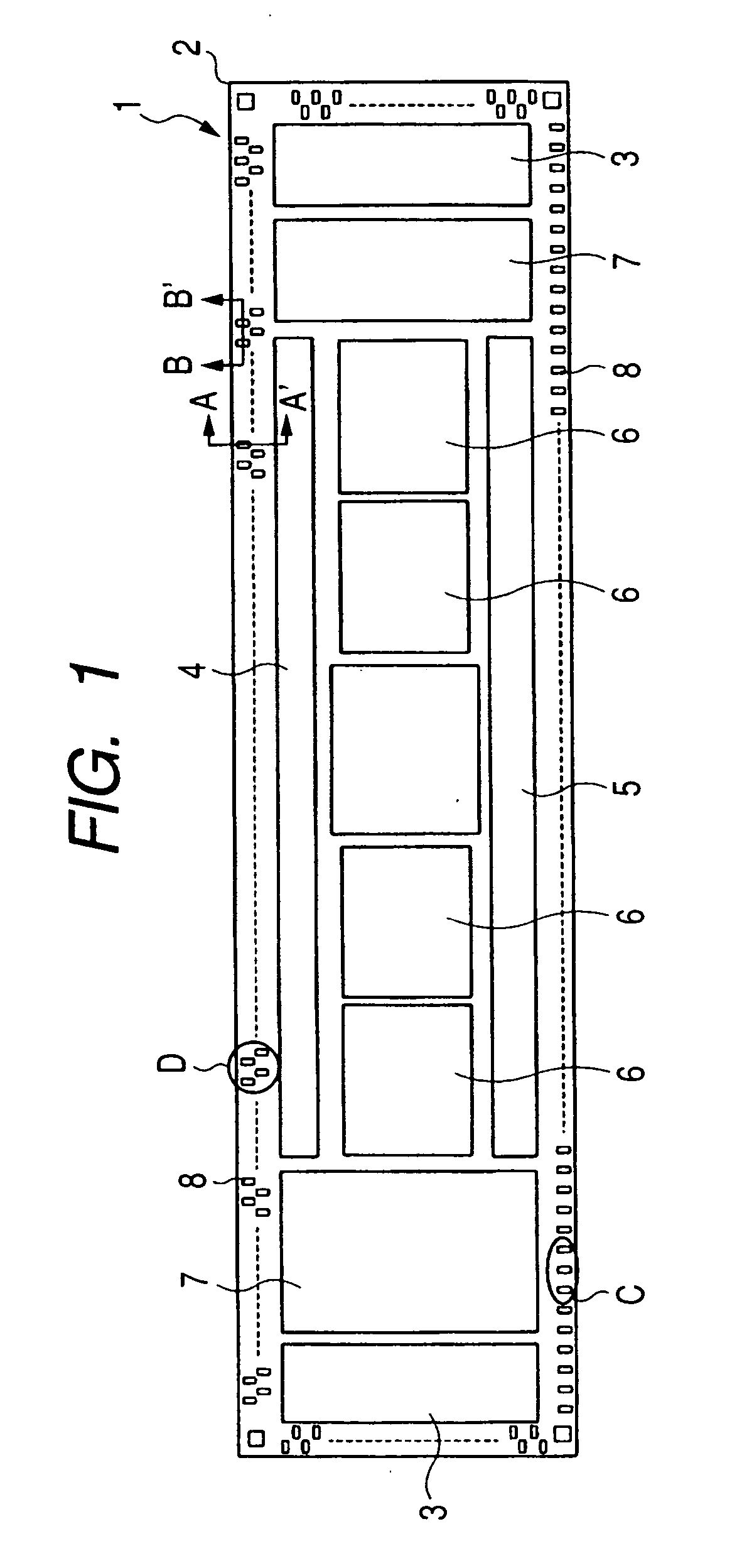
[0047]FIG. 1 is a plan view showing the structure of a semiconductor chip 1 (semiconductor device) according to the first embodiment. The semiconductor chip 1 according to the first embodiment is a driver for an LCD. Referring to FIG. 1, the semiconductor chip 1 has a semiconductor substrate 2 which takes the form of, for example, an elongated rectangle, and for example, an LCD driver which drives a liquid crystal display is formed on its main surface. This driver has the function of controlling the orientations of liquid crystal molecules by supplying voltage to each pixel in a cell array constituting the LCD and includes gate drive circuits 3, a source drive circuit 4, a liquid crystal circuit 5, graphic RAMs (Random Access Memories) 6, and peripheral circuits 7.

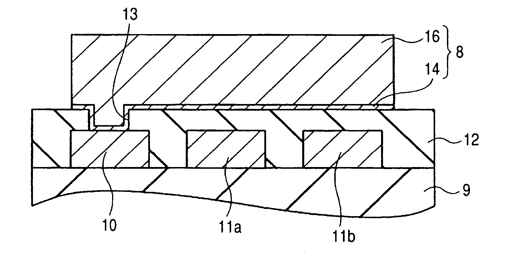
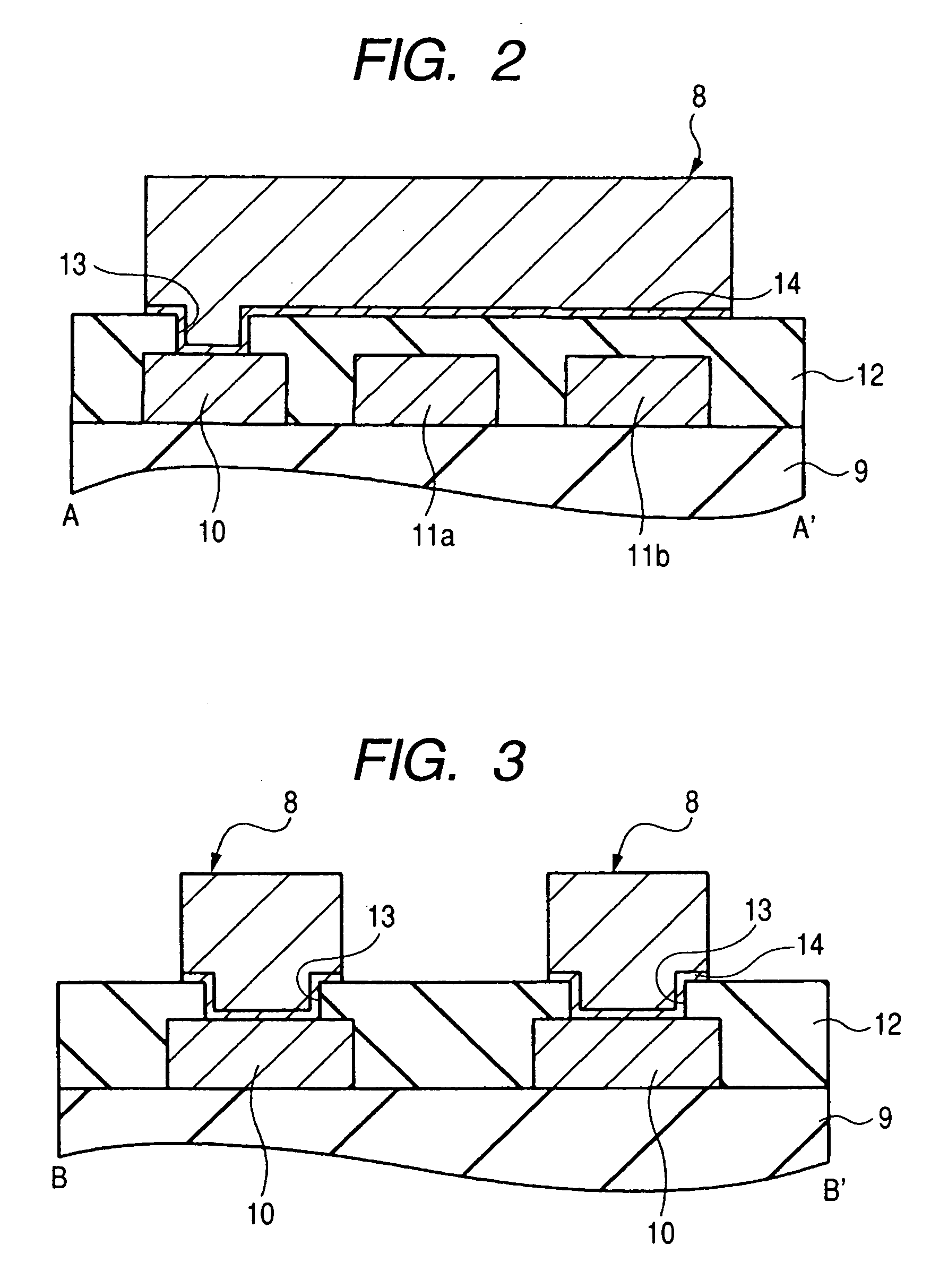
[0048] In the vicinity of the periphery of the semiconductor chip 1, a plurality of bump electrodes 8 are arranged at regular intervals along the periphery of the semiconductor chip 1. These bump electrodes 8 lie over act...

second embodiment

[0076] The second embodiment concerns a semiconductor device with wide layout latitude which optimizes pad positions regardless of bump electrode positions.

[0077]FIG. 20 is a fragmentary plan view of a semiconductor chip according to the second embodiment. Referring to FIG. 20, a pad 10 is connected with a pad connection portion 8a as a part of a bump electrode 8 through an opening 13 made in a surface protective film 12. The bump electrode 8 consists of: a pad connection portion 8a to be connected with the pad 10; a terminal connection portion 8c to be connected with a terminal of a packaging substrate; and a wiring portion 8b which connects the pad connection portion 8a and the terminal connection portion 8c. A conventional bump electrode consists of only a terminal connection portion which is connected with a pad. In other words, in a conventional bump electrode, the terminal connection portion also functions as a pad connection portion, which means that the pad connection porti...


PUM


Abstract

A semiconductor device manufacturing technique which allows reduction of semiconductor chip size. First, a pad and other wires are formed over an insulating film. A surface protective film is formed over the insulating film including the pad and wires, and an opening is made in the surface protective film. The opening lies over the pad and exposes a surface of the pad. A bump electrode is formed over the surface protective film including the opening. Here, the pad is smaller than the bump electrode. Consequently, the wires are arranged just beneath the bump electrode in the same layer as the pad 10. In other words, the wires are arranged in space which becomes available because the pad is small enough.

Description

BACKGROUND OF THE INVENTION [0001] The present invention relates to a semiconductor device and a method of manufacturing the same and more particularly to a technique which is useful for semiconductor devices used in LCD (Liquid Crystal Display) drivers. [0002] Japanese Unexamined Patent Publication No. Hei 10 (1998)-233507 discloses a technique which reduces the chip area and achieves production efficiency improvement and cost reduction regarding semiconductor integrated circuits such as driver ICs with many output pads and electronic circuit devices such as electronic clocks. [0003] Concretely, an output pads is placed over a drive transistor to be connected with the output pad or over a logic circuit so that they overlap each other as seen in a plan view. Furthermore, not only aluminum wires but also bump electrodes or barrier metals are used for semiconductor device wiring interconnection. Also, in a case that a semiconductor integrated circuit is electrically bonded over a prin...

Claims


Application Information

Patent Timeline
Patent Type & Authority Applications(United States)
IPC IPC(8): H01L31/0203H01L21/44
CPCG02F1/13452H01L23/3157H01L2924/1306H01L2924/00011H01L2224/73204H01L2224/293H01L2224/2929H01L2924/00014H01L2924/0001H01L2224/45124H01L23/48H01L2924/014H01L2924/01006H01L2924/01005H01L24/13H01L2924/19043H01L2924/14H01L23/522H01L24/11H01L24/83H01L2224/0401H01L2224/0603H01L2224/1147H01L2224/13099H01L2224/1403H01L2224/83851H01L2924/01013H01L2924/01015H01L2924/01022H01L2924/01029H01L2924/01033H01L2924/01046H01L2924/01074H01L2924/01078H01L2924/01079H01L2924/01082H01L2924/04941H01L2924/00H01L2224/48H01L2224/29075H01L2924/15788H01L2224/14104H01L2224/023H01L2924/00012H01L21/28H01L2224/13027H01L2224/16105H01L2224/73203H01L21/50H01L23/485H01L27/124H01L2021/60232H01L2021/60262
Inventor YOSHIOKA, AKIHIKOSUZUKI, SHINYA
Owner RENESAS TECH CORP
Why Eureka
Try Eureka