
Eureka
For R&D, Eureka makes reading and utilizing patents & technical documents easy.
Eureka AIR
Designed for self-driven R&D workflows. Generate viable solutions, solve complex R&D challenges, empower your innovation with AI.

Eureka Materials
Designed for material experts only. Revolutionize your material R&D, from search, analyze, to developing new materials.

TechResearch
Generate reliable direction feasibility study reports for your R&D in just a few steps.

TechSeek
Discover and master advanced knowledge NOW. Basics, ideas, possibilities, all at once.

TechMind
As an expert in R&D Theories, TechMind can generates customized viable solutions instantly.

TechRisk
Analyze your overall solution with one click, know your potential R&D risks in advance.

TechMonitor
Get weekly tech updates, stay abreast of the latest tech innovations and key insights.
Plasma display panel
- Summary
- Abstract
- Description
- Claims
- Application Information
AI Technical Summary
Problems solved by technology
Method used
Image

Examples
Embodiment Construction
[0035] The present embodiments will now be described more fully with reference to the accompanying drawings, in which exemplary embodiments are shown.
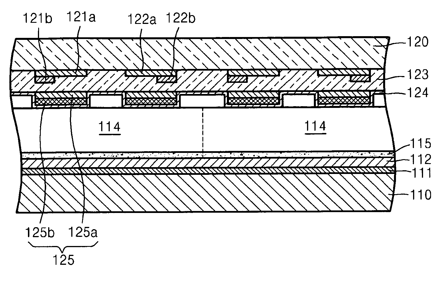
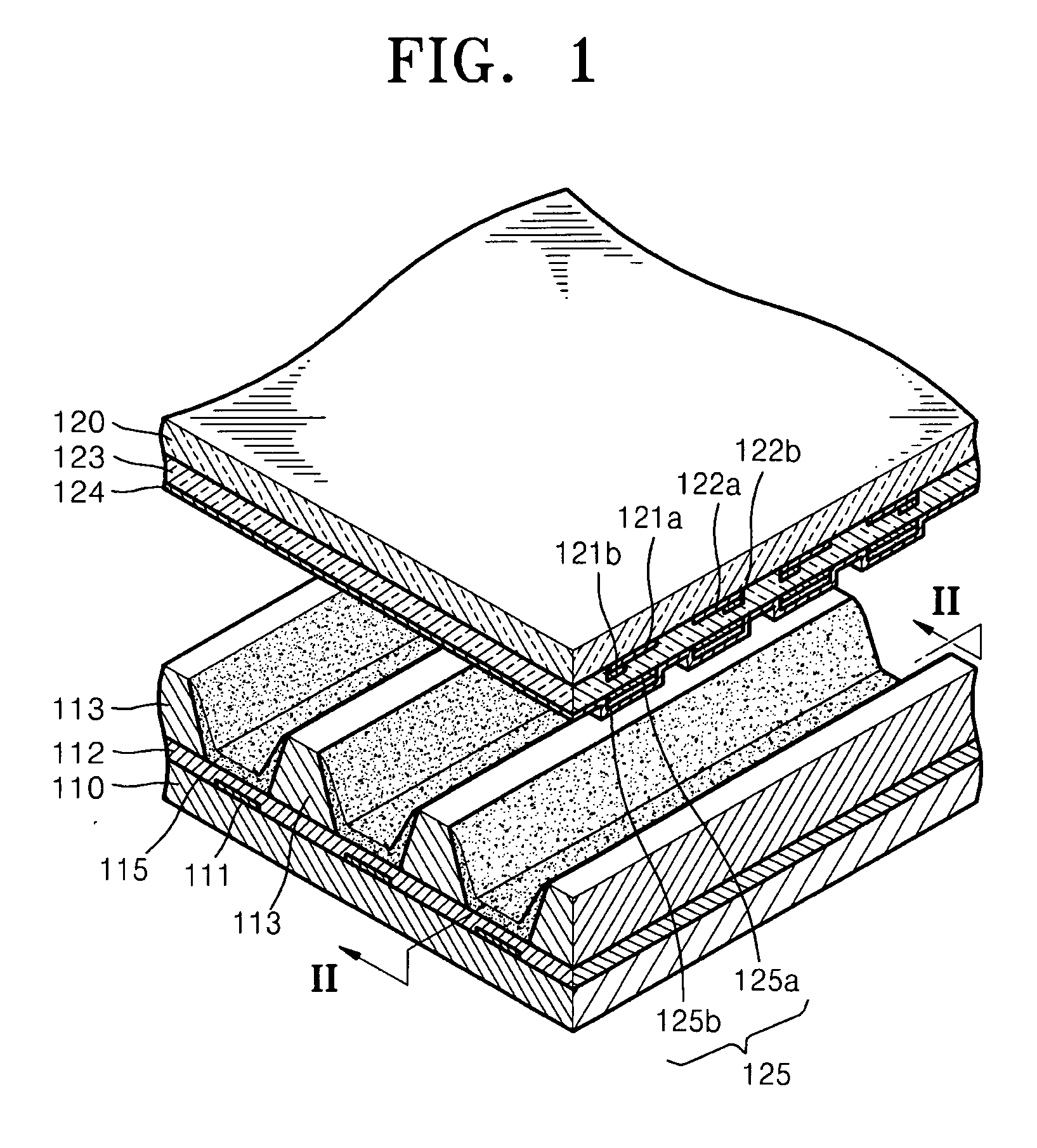
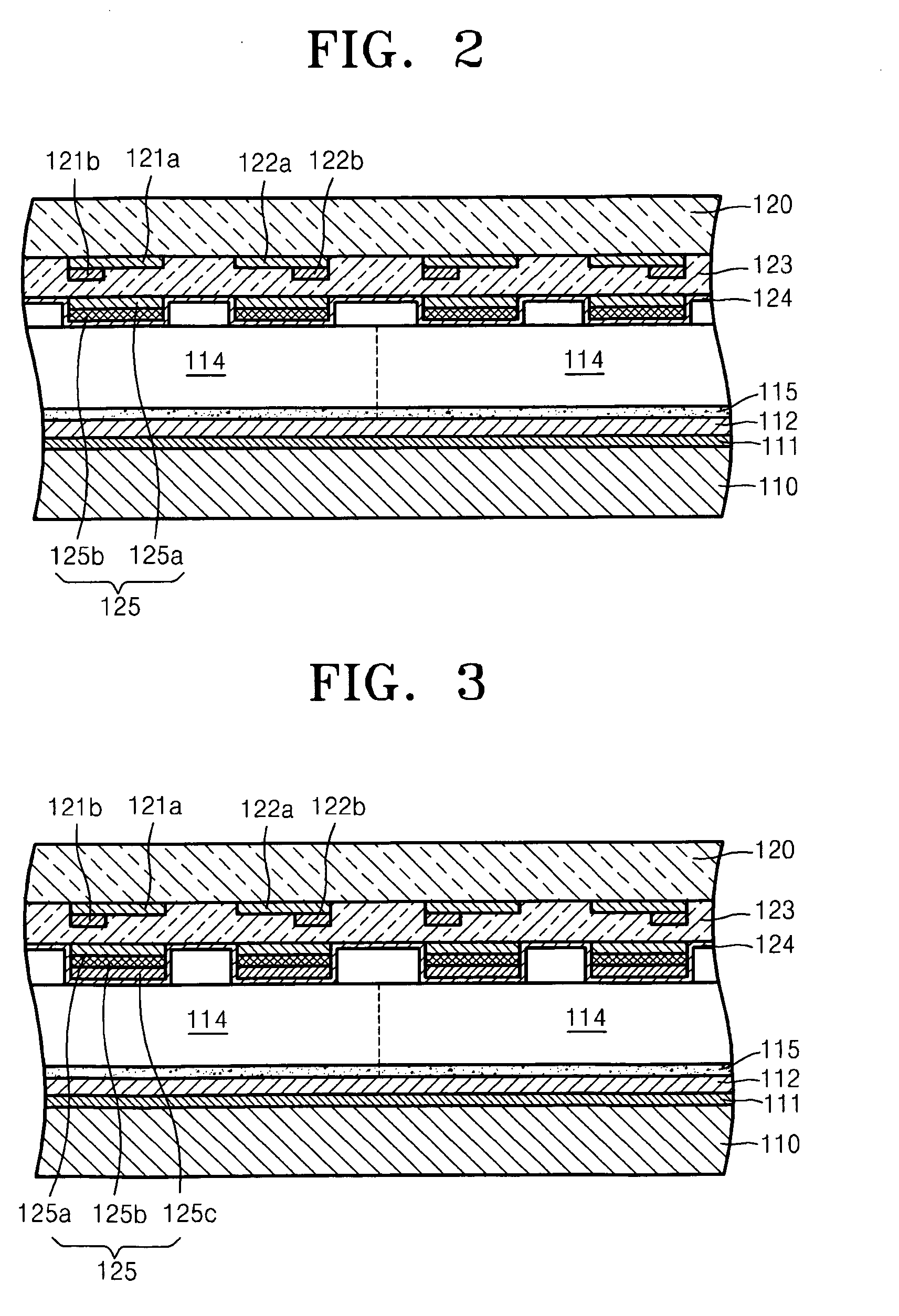
[0036]FIG. 1 is an exploded perspective view of a plasma display panel (PDP) according to an embodiment. FIG. 2 is a cross-sectional view of the PDP of FIG. 1 taken along line II-II in FIG. 1. Referring to FIGS. 1 and 2, the PDP comprises a first substrate 110, a second substrate 120, barrier ribs 113, X and Y sustain electrodes 121 and 122 (see FIG. 6A), a first dielectric layer 112, address electrodes 111, a second dielectric layer 123, phosphor layers 115, a protective layer 124, and electron emission members 125.
[0037] The first substrate 110 and the second substrate 120 are separated by a predetermined distance and face each other to form a discharge space. The second substrate 120 is formed of a transparent material such as glass to transmit visible light. However, the present embodiments are not limited thereto. For example, t...
PUM
 Abstract
Description
Claims
Application Information
 - R&D Engineer
- R&D Manager
- IP Professional
- Industry Leading Data Capabilities
- Powerful AI technology
- Patent DNA Extraction
Browse by: Latest US Patents, China's latest patents, Technical Efficacy Thesaurus, Application Domain, Technology Topic, Popular Technical Reports.
© 2024 PatSnap. All rights reserved.Legal|Privacy policy|Modern Slavery Act Transparency Statement|Sitemap|About US| Contact US: help@patsnap.com